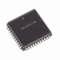
DS2143QN Maxim Integrated Products, DS2143QN Datasheet - Page 23

DS2143QN
Manufacturer Part Number
DS2143QN
Description
IC CONTROLLER E1 5V LP 44-PLCC
Manufacturer
Maxim Integrated Products
Datasheet
1.DS2143Q.pdf
(44 pages)
Specifications of DS2143QN
Controller Type
E1 Controller
Interface
Parallel/Serial
Voltage - Supply
4.5 V ~ 5.5 V
Current - Supply
10mA
Operating Temperature
-40°C ~ 85°C
Mounting Type
Surface Mount
Package / Case
44-LCC, 44-PLCC
Lead Free Status / RoHS Status
Contains lead / RoHS non-compliant
Available stocks
Company
Part Number
Manufacturer
Quantity
Price
Company:
Part Number:
DS2143QN+
Manufacturer:
Maxim Integrated Products
Quantity:
135
Company:
Part Number:
DS2143QN/T&R
Manufacturer:
Maxim Integrated
Quantity:
10 000
EBCR1: E-BIT COUNT REGISTER 1 (Address=04 Hex)
EBCR2: E-BIT COUNT REGISTER 2 (Address=05 Hex)
E-bit Count Register 1 (EBCR1) is the most significant word and EBCR2 is the least significant word of
a 16-bit counter that records Far End Block Errors (FEBE) as reported in the first bit of frames 13 and 15
on E1 lines running with CRC4 multiframe. These count registers will increment once each time the
received E-bit is set to 0. Since the maximum E-bit count in a 1-second period is 1000, this counter
cannot saturate. The counter is disabled during loss of sync at either the FAS or CRC4 level; it will
continue to count if loss of sync occurs at the CAS level.
6.0 Sa DATA LINK CONTROL AND OPERATION
The DS2143 provides for access to the proposed E1 performance monitor data link in the Sa bit positions.
The device allows access to the Sa bits either via a set of two internal registers (RNAF and TNAF) or via
two external pins (RLINK and TLINK).
On the receive side, the Sa bits are always reported in the internal RNAF register (see Section 11 for more
details). All five Sa bits are always output at the RLINK pin. See Section 13 for detailed timing. Via
RCR2, the user can control the RLCLK pin to pulse during any combination of Sa bits. This allows the
user to create a clock that can be used to capture the needed Sa bits.
On the transmit side, the individual Sa bits can be either sourced from the internal TNAF register
(TCR1.6=0) or from the external TLINK pin. Via TCR2, the DS2143 can be programmed to source any
combination of the additional bits from the TLINK pin. If the user wishes to pass the Sa bits through the
DS2143 without them being altered, then the device should be set up to source all 5 Sa bits via the
TLINK pin and the TLINK pin should be tied to the TSER pin. Please see the timing diagrams and the
transmit data flow diagram in Section 13 for examples.
7.0 SIGNALING OPERATION
The Channel Associated Signaling (CAS) bits embedded in the E1 stream can be extracted from the
receive stream and inserted into the transmit stream by the DS2143. Each of the 30 channels has 4
signaling bits (A/B/C/D) associated with it. The numbers in parenthesis () are the channel associated with
a particular signaling bit. The channel numbers have been assigned as described in the CCITT documents.
For example, channel 1 is associated with timeslot 1 and channel 30 is associated with timeslot 31. There
is a set of 16 registers for the receive side (RS1 to RS16) and 16 registers on the transmit side (TS1 to
TS16). The signaling registers are detailed below.
(MSB)
EB15
EB7
SYMBOL
EB15
EB0
EB14
EB6
POSITION
EBCR1.7
EBCR2.0
EB13
EB5
EB12
EB4
MSB of the E-Bit error count.
LSB of the E-Bit error count.
NAME AND DESCRIPTION
23 of 44
EB11
EB3
EB10
EB2
EB1
EB9
EB0
EB8
(LSB)
DS2143/DS2143Q
EBCR2
EBCR1


