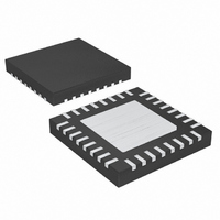
MAX3421EETJ+T Maxim Integrated Products, MAX3421EETJ+T Datasheet - Page 17

MAX3421EETJ+T
Manufacturer Part Number
MAX3421EETJ+T
Description
IC USB PERIPH/HOST CNTRL 32TQFN
Manufacturer
Maxim Integrated Products
Datasheet
1.MAX3421EETJ.pdf
(32 pages)
Specifications of MAX3421EETJ+T
Controller Type
USB Peripheral Controller
Interface
USB/Serial
Voltage - Supply
3 V ~ 3.6 V
Current - Supply
15mA
Operating Temperature
-40°C ~ 85°C
Mounting Type
Surface Mount
Package / Case
32-TQFN Exposed Pad
For Use With
MAX3421EVKIT-1+ - EVAL KIT FOR MAX3421E
Lead Free Status / RoHS Status
Lead free / RoHS Compliant
Drive RES low to put the MAX3421E into a chip reset. A
chip reset sets all registers to their default states,
except for PINCTL (R17), USBCTL (R15), and SPI logic.
All FIFO contents are unknown during chip reset. Bring
the MAX3421E out of chip reset by driving RES high.
The RES pulse width can be as short as 200ns. See the
Device Reset section for a description of the resets
available on the MAX3421E.
The MAX3421E INT output pin signals when a USB
event occurs that requires the attention of the SPI mas-
ter. INT can also be configured to assert when any of
the general-purpose inputs (GPIN0–GPIN7) are activat-
ed (see the GPIN7–GPIN0 section for more details).
The SPI master must set the IE bit in the CPUCTL (R16)
register to activate INT. When the IE bit is cleared, INT
is inactive (open for level mode, high for negative edge,
low for positive edge). INT is inactive upon power-up or
after a chip reset (IE = 0).
The INT pin can be a push-pull or open-drain output.
Set the INTLEVEL bit of the PINCTL (R17) register high
to program the INT output pin to be an active-low level
open-drain output. An external pullup resistor to V
required for this setting. In level mode, the MAX3421E
drives INT low when any of the interrupt flags are set. If
multiple interrupts are pending, INT goes inactive only
when the SPI master clears the last active interrupt
request bit (Figure 12). The POSINT bit of the PINCTL
(R17) register has no effect on INT in level mode.
Clear the INTLEVEL bit to program INT to be an edge
active push-pull output. The active edge is programma-
ble using the POSINT bit of the PINCTL (R17) register.
In edge mode, the MAX3421E produces an edge refer-
Figure 12. Behavior of the INT Pin for Different INTLEVEL and
POSINT Bit Settings
INTLEVEL = 1
INTLEVEL = 0
INTLEVEL = 0
(1) WIDTH DETERMINED BY TIME TAKEN TO CLEAR THE IRQ.
(2) WIDTH DETERMINED BY PULSEWID1 AND PULSEWID0 BITS IN CPUCTL (R16) REGISTER.
POSINT = X
POSINT = 0
POSINT = 1
SINGLE
IRQ
(1)
CLEAR
IRQ
______________________________________________________________________________________
FIRST IRQ
ACTIVE
(2)
SECOND
ACTIVE
IRQ
FIRST IRQ,
IRQ STILL
SECOND
ACTIVE
CLEAR
,
USB Peripheral/Host Controller
PENDING
CLEAR
LAST
IRQ
INT
INT
INT
RES
INT
L
is
enced to V
or when an interrupt request is cleared and others are
pending (Figure 12). Set the POSINT bit in the PINCTL
(R17) register to make INT active high, and clear the
POSINT bit to make INT active low. The PULSEWID1
and PULSEWID0 bits in the CPUCTL (R16) register
control the pulse width of INT in edge mode as shown
in Table 4.
The SPI master samples GPIN3–GPIN0 states by read-
ing bit 7 through bit 4 of the IOPINS1 (R20) register.
GPIN7–GPIN4 states are sampled by reading bit 7
through bit 4 of the IOPINS2 (R21) register. Writing to
these bits has no effect.
Three registers, operational in both peripheral and host
mode, control eight interrupt requests from the
GPIN7–GPIN0 inputs. The GPINIRQ (R22) register con-
tains the interrupt request flags for the eight GPIN
inputs. The GPINIEN (R23) register contains individual
interrupt enable bits for the eight GPIN interrupts. The
GPINPOL (R24) register controls the edge polarity for
the eight GPIN interrupts. The eight GPIN interrupts are
added into the MAX3421E interrupt system and appear
on the INT output pin if enabled and asserted. It is also
possible to separate the GPIN interrupts and make them
available on the GPX output pin by setting SEPIRQ = 1.
This provides lower latency interrupt service since the
source of the interrupt on the GPX output is known, and
only the GPINIRQ register needs to be checked to
determine the interrupt source. Note that the GPINPOL
bits control the edge sensitivity of the GPIN transitions
as they set an internal “interrupt pending” flip-flop, not
the INT output pin. The INT pin output characteristics
are determined by the INTLEVEL and POSINT register
bits, as in the MAX3420E. If the GPX pin is configured
as the GPIN INT pin, its output characteristics are the
same as programmed for the INT pin.
Table 4. Pulse Width of INT Output
Configured by PULSEWID1 and
PULSEWID0
PULSEWID1
0
0
1
1
L
with SPI Interface
any time an interrupt request is activated,
PULSEWID0
0
1
0
1
INT PULSE WIDTH (µs)
GPIN7–GPIN0
10.6
5.3
2.6
1.3
17


