Z16C3010ASC Zilog, Z16C3010ASC Datasheet
Z16C3010ASC
Specifications of Z16C3010ASC
Available stocks


Related parts for Z16C3010ASC


Z16C3010ASC Summary of contents
Page 1
... Z16C30 CMOS USC Universal Serial Controller Product Specification DS007902-0708 ® Copyright ©2008 by Zilog , Inc. All rights reserved. www.zilog.com ...
Page 2
... TECHNOLOGY DESCRIBED HEREIN OR OTHERWISE. The information contained within this document has been verified according to the general principles of electrical and mechanical engineering. Z8, Z8 Encore!, Z8 Encore! XP, Z8 Encore! MC, Crimzon, eZ80, and ZNEO are trademarks or registered trademarks of Zilog, Inc. All other product or service names are the property of their respective owners. DS007902-0708 ...
Page 3
Revision History Each instance in Revision History reflects a change to this document from its previous revision. For more details, refer to the corresponding pages and appropriate links in the table below. Date Revision Level July 2008 02 Jan 2000 ...
Page 4
Table of Contents Architectural Overview . . . . . . . . . . . . . . . . . . . . . . . . . . . . . . . . . . . ...
Page 5
... Architectural Overview Features The key features of Zilog’s Z16C30 device include: • Two Independent 0-to-10 Mbps Full-Duplex Channels, each with Two Baud Rate Gener- ators and One digital phase-locked loop (DPLL) for Clock Recovery • 32-byte Data FIFO’s for each Receiver and Transmitter • ...
Page 6
... FIFO’s for each receiver and transmitter Zilog now offers a high speed version of the USC with improved bus bandwidth. CPU bus accesses have been shortened from 160 ns per access to 110 ns per access. The USC has a transmit and receive clock range MHz (20 MHz when using the DPLL, BRG, or CTR) and data transfer rates as high as 10 Mbits/sec full duplex ...
Page 7
Table 1. Power connection conventions Connection Power Ground To Other Channel CPU DS007902-0708 Circuit V CC GND Receive DMA Control Receive FIFO (32 byte) I/O and Interrupt Device Control Status Channel Control Transmit FIFO (32 byte) Transmit DMA Control Figure ...
Page 8
Pin Description Address/ Data Bus Bus Timing Control Interrupt Ground DS007902-0708 TxDA AD0 RxDA AD1 TxCA AD2 RxCA AD3 CTSA AD4 AD5 DCDA RxREQA AD6 RxACKA AD7 TxREQA AD8 TxACKA AD9 INTA AD10 IEIA AD11 IEOA AD12 AD13 TxDB RxDB ...
Page 9
RxACKA INTA IEIA IEOA GND V CC AD0 AD1 AD2 AD3 AD4 AD5 AD6 AD7 GND V CC RXREQA 26 27 DS007902-0708 1 68-Pin PLCC Figure 3. Z16C30 68-Pin PLCC Pin Assignments ...
Page 10
TXACKB 80 PITACK 81 R RESET D/C 92 A/B 93 ...
Page 11
The 8-bit bus with separate address is selected by setting BCR bit and, during the BCR write, forcing AD15 and forcing AD14–AD8 to 0. The multiplexed bus is selected for the USC if there ...
Page 12
PITACK Pulsed Interrupt Acknowledge (input, active Low)— signal that indicates that an interrupt acknowledge cycle is in progress. The device is capa- ble of returning an interrupt vector that may be encoded with the type of interrupt pending during this ...
Page 13
RxACKA, RxACKB Receive Acknowledge (inputs or outputs, active Low)— mary function of these signals is to perform fly-by DMA transfers from the receive FIFOs. They may also be used as bit inputs or outputs. TxDA, TxDB Transmit Data (outputs, active ...
Page 14
Electrical Characteristics Table 2. Absolute Maximum Ratings Symbol STG Voltage on all pins with respect to GND. † See Ordering Information Stresses greater than those listed under Absolute Maximum Ratings may cause permanent damage ...
Page 15
From Pin Capacitance Table 3. Capacitance Symbol Parameter C Input Capacitance IN C Output Capacitance OUT CI/O Bidirectional Capacitance Note MHz over specified temperature range. Miscellaneous Transistor Count: 174,000 Temperature Ratings Standard = ...
Page 16
DC Characteristics Table 4. Z16C30 DC Characteristics Symbol Parameter V Input High Voltage 2 Input Low Voltage –0 Output High OH1 Voltage V Output High OH2 Voltage V Output Low OL Voltage I Input Leakage IL ...
Page 17
Table 5. Z16C30 AC Characteristics (Continued) No Symbol Parameter 12 TsCS(AS Rise Setup Time 13 ThCS(AS Rise Hold Time 14 TsADD(AS) Direct Address to AS Rise Setup Time 15 ThADD(AS) Direct Address to AS ...
Page 18
Table 5. Z16C30 AC Characteristics (Continued) No Symbol Parameter 35 TdRD(DRz) RD Rise to Data Float Delay 36 TdRDf(RRQ) RD Fall to RxREQ Inactive Delay 37 TdRDr(RRQ) RD Rise to RxREQ Active Delay 38 TwWRl WR Low Width 39 TwWRh ...
Page 19
Table 5. Z16C30 AC Characteristics (Continued) No Symbol Parameter 59 ThCS(WR Fall Hold Time 60 TsADD(WR) Direct Address to WR Fall Setup Time 61 ThADD(WR) Direct Address to WR Fall Hold Time 62 TsSIA(WR) SITACK to WR ...
Page 20
Table 5. Z16C30 AC Characteristics (Continued) No Symbol Parameter 81 TsIEI(DSI) IEI to DS Fall (INTACK) Setup Time 82 ThIEI(DSI) IEI to DS Rise (INTACK) Hold Time 83 TdIEI(IEO) IEI to IEO Delay 84 TdAS(IEO) AS Rise (Intack) to IEO ...
Page 21
Table 5. Z16C30 AC Characteristics (Continued) No Symbol Parameter 103 TsIEI(PIA) IEI to PITACK Fall Setup Time 104 ThIEI(PIA) IEI to PITACK Rise Hold Time 105 TdPIA(IEO) PITACK Fall to IEO Delay 106 TdPIA(INT) PITACK Fall to INT Inactive Delay ...
Page 22
Table 5. Z16C30 AC Characteristics (Continued) No Symbol Parameter 123 TdTAKr(RDY) TxACK Rise to RDY Rise Delay Notes 1. Direct address is any of A/B, D/C, or AD15–AD8 used as an address bus. 2. The parameter applies only when AS ...
Page 23
STB RxACK AD15–AD0 RxREQ WAIT/RDY (Wait) WAIT/RDY (Ready) Note: STB is any of DS, RD, WR, PITACK, RxACK, or TxACK DS007902-0708 112 1 1 Figure 7. Bus Cycle Timing 120 79 Figure 8. DMA Read Cycle ...
Page 24
TxACK AD15–AD0 TxREQ WAIT/RDY (Wait) WAIT/RDY (Ready) DS007902-0708 122 Figure 9. DMA Write Cycle Z16C30 Product Specification 123 Electrical Characteristics 20 ...
Page 25
CS 12 A/B, D/C 14 ACK R/W DS AD15–AD0 18 RxREQ WAIT/RDY (Wait) WAIT/RDY (Ready) DS007902-0708 116 Figure 10. Multiplexed DS Read Cycle ...
Page 26
CS 12 A/B, D/C 14 SITACK R/W DS AD15–AD0 18 TxREQ WAIT/RDY (Wait) WAIT/RDY (Ready) DS007902-0708 116 Figure 11. Multiplexed DS Write Cycle ...
Page 27
A/B, D/C 14 SITACK AD15–AD0 18 RxREQ WAIT/RDY (Wait) WAIT/RDY (Ready) DS007902-0708 119 79 Figure 12. Multiplexed RD Read Cycle ...
Page 28
CS 12 A/B, D/C 14 SITACK AD15–AD0 18 TxREQ WAIT/RDY (Wait) WAIT/RDY (Ready) DS007902-0708 117 Figure 13. Multiplexed WR Write Cycle ...
Page 29
CS 12 A/B, D/C 14 SITACK AD15–AD0 18 TxREQ WAIT/RDY (Wait) WAIT/RDY (Ready) DS007902-0708 117 Figure 14. Nonmultiplexed DS Read Cycle ...
Page 30
CS 46 A/B, D/C 48 SITACK 50 R AD15–AD0 TxREQ WAIT/RDY (Wait) WAIT/RDY (Ready) DS007902-0708 116 Figure 15. Nonmultiplexed DS Write Cycle ...
Page 31
CS 52 A/B, D/C 54 SITACK 56 RD AD15–AD0 RxREQ WAIT/RDY (Wait) WAIT/RDY (Ready) WAIT/RDY (Ready) DS007902-0708 119 Figure 16. Nonmultiplexed RD Read Cycle ...
Page 32
CS 58 A/B, D/C 60 SITACK 62 WR AD15–AD0 TxREQ WAIT/RDY (Wait) WAIT/RDY (Ready) DS007902-0708 117 Figure 17. Nonmultiplexed WR Write Cycle ...
Page 33
AS 2 SITACK 16 DS AD15–AD0 18 WAIT/RDY (Wait) WAIT/RDY (Ready) IEI IEO 83 INT Figure 18. Multiplexed DS Interrupt Acknowledged Cycle DS007902-0708 ...
Page 34
AS 2 SITACK 16 RD AD15–AD0 18 19 WAIT/RDY (Wait) WAIT/RDY (Ready) IEI IEO 83 INT Figure 19. Multiplexed RD Interrupt Acknowledge Cycle DS007902-0708 ...
Page 35
AS 2 PITACK AD15–AD0 18 WAIT/RDY (Wait) WAIT/RDY (Ready) IEI IEO 83 INT Figure 20. Multiplexed Pulsed Interrupt Acknowledge Cycle DS007902-0708 100 19 109 88 110 79 107 103 105 106 ...
Page 36
SITACK DS AD15–AD0 WAIT/RDY (Wait) WAIT/RDY (Ready) IEI IEO 83 INT Figure 21. Nonmultiplexed DS Interrupt Acknowledge Cycle DS007902-0708 111 ...
Page 37
SITACK RD AD15–AD0 WAIT/RDY (Wait) WAIT/RDY (Ready) IEI 81 IEO 83 111 INT Figure 22. Nonmultiplexed RD Interrupt Acknowledge Cycle DS007902-0708 ...
Page 38
SITACK PITACK AD15–AD0 WAIT/RDY (Ready) IEI IEO INT WAIT/RDY (Wait) Figure 23. Nonmultiplexed Pulsed Interrupt Acknowledge Cycle DS007902-0708 96 100 79 107 103 83 105 106 109 110 Z16C30 ...
Page 39
PITACK (2-Pulse) AD15–AD0 18 WAIT/RDY (Ready) WAIT/RDY (Wait) IEI IEO 83 INT DS007902-0708 100 19 19 107 110 103 105 106 Figure 24. Multiplexed Double-Pulse Intack Cycle ...
Page 40
PITACK (2-Pulse) AD15–AD0 WAIT/RDY (Ready) WAIT/RDY (Wait) IEI IEO 83 INT Figure 25. Nonmultiplexed Double-Pulse Intack Cycle DS007902-0708 100 107 110 103 105 106 Z16C30 Product ...
Page 41
AC Characteristics Table 6 lists Z16C30 General Timing. Table 6. Z16C30 General Timing No Symbol Parameter 1 TsRxD(RxCr) RxD to RxC Rise Setup Time (x1 Mode) 2 ThRxD(RxCr) RxD to RxC Rise Hold Time (x1 Mode) 3 TsRxd(RxCf) RxD to ...
Page 42
RxC, TxC Receive RxEQ Request RxC as Receiver Output INT RxC, TxC Transmit TxREQ TxC as Transmitter Output CTS, DCD, TxREQ, RxREQ Note: CLK is RxC or TxC when supplying DPLL, BRG, or CTR clock. Table 7 lists Z16C30 System ...
Page 43
Table 7. Z16C30 System Timing No Symbol Parameter 1 TdRxC(REQ) RxC Rise to RxREQ Valid Delay 2 TdRxC(RxC) TxC Rise to RxC as Receiver Output Valid Delay 3 TdRxC(INT) RxC Rise to INT Valid Delay 4 TdTxC(REQ) TxC Fall to ...
Page 44
Address: None D15 D14 D13 D12 D11 D10 D9 * Must be programmed as 0. Data Path Both the transmitter and the receiver in the channel are actually microcoded serial proces- sors. As the data shifts through the transmit or ...
Page 45
Functional Description The functional capabilities of the USC are described from two different points of view data communications device, it transmits and receives data in a wide variety of data communications protocols microprocessor peripheral, the USC ...
Page 46
CRC on either an underrun or at the end of a programmed message length. This mode is identical to monosync mode except that character synchroni- Bisync Mode— zation requires two successive characters for synchronization. The two ...
Page 47
In NRZ represented by a High level for the duration of the bit cell and NRZ— represented by a Low level for the duration of the bit cell. Data is inverted from NRZ. NRZB— ...
Page 48
Data 1 NRZ NRZB NRZI-M NRZI-S BI-PHASE-M BIPHASE-S BIPHASE-L DIFFERENTIAL BIPHASE-L Differential Biphase-Level— tion at the center of the bit cell, with the opposite polarity from the transition at the center of the preceding bit cell represented ...
Page 49
FIFO. This allows DMA transfer of data to proceed without CPU intervention at the end of a received message, as the values in the FIFO allow the CPU to determine message boundaries in memory. Similarly, ...
Page 50
Clock Multiplexer The clock multiplexer in each channel selects the clock source for the various blocks in the channel and selects an internal clock signal to potentially be sent to either the RxC or TxC pin. Test Modes The USC ...
Page 51
In the USC, the IP bit signals that an interrupt request is being serviced IUS is set, all interrupt sources of lower priority within the channel and external to the channel are pre- vented from requesting interrupts. The ...
Page 52
The first write to the USC, after a hardware reset, programs the BCR. From that time on, the normal channel registers may be accessed. No specific address need be presented to ...
Page 53
Any Transaction and Including BCR W rite Non-Multiplexed BCR Write Transaction BCR[2]=0 BCR[2]=0 BCR[15]=1 BCR[15]=0 8-Bit With 8-Bit Without Separate Separate Address Address Note: The presence of one transaction with an /AS active between reset ...
Page 54
Table 9. Register Address List Address A4–A0 00000 00001 00010 00011 00110 00111 01000 01001 01010 01011 01100 01101 01110 01111 1X000 10001 10010 10011 10100 10101 10110 10111 1X000 11001 11010 11011 11100 11101 11110 11111 XXXXX DS007902-0708 CCAR ...
Page 55
Control Registers DS007902-0708 Figure 30. Channel Command/Address Register Z16C30 Product Specification 51 Functional Description ...
Page 56
Address: 00001 D15 D14 D13 D12 D11 D10 ...
Page 57
Address: 00001 D15 D14 D13 D12 D11 D10 Asynchronous 0 0 16X Data Rate 0 1 32X Data Rate 1 0 64X Data Rate 1 1 Reserved 0 0 One Stop Bit 0 1 Two ...
Page 58
Address: 00001 D15 D14 D13 D12 D11 D10 Figure 33. Channel Mode Register, External Sync Mode Address: 00001 D15 D14 D13 D12 D11 D10 Figure 34. Channel Mode Register, Isochronous Mode DS007902-0708 D9 ...
Page 59
Address: 00001 D15 D14 D13 D12 D11 D10 One Stop Bit 0 1 Two Stop Bits Tx Stop Bits Stop Bit 1 1 Reserved Figure 35. Channel Mode Register, Asynchronous Mode with ...
Page 60
Address: 00001 D15 D14 D13 D12 D11 D10 Figure 36. Channel Mode Register, Monosync Mode DS007902-0708 Transmitter 0 Monosync Mode ...
Page 61
Address: 00001 D15 D14 D13 D12 D11 D10 SYN1 0 1 SYN0/SYN1 1 0 CRC/SYN1 1 1 CRC/SYN0/SYN1 DS007902-0708 Transmitter Bisync Mode Tx Underrun Condition Figure ...
Page 62
Address: 00001 D15 D14 D13 D12 D11 D10 Abort 0 1 Extended Abort 1 0 Flag 1 1 CRC/Flag DS007902-0708 Disabled 0 1 One Byte, No ...
Page 63
Address: 00001 D15 D14 D13 D12 D11 D10 Transparent Bisync 0 0 SYN 0 1 DLE/SYN 1 0 CRC/SYN 1 1 CRC/DLE/SYN Figure 39. Channel Mode Register, Transparent Bisync Mode DS007902-0708 ...
Page 64
Address: 00001 D15 D14 D13 D12 D11 D10 16X Data Rate 0 1 32X Data Rate 1 0 64X Data Rate 1 1 Reserved DS007902-0708 ...
Page 65
Address: 00001 D15 D14 D13 D12 D11 D10 DS007902-0708 Transmitter 1 802.3 Mode Figure 41. Channel Mode Register, 802.3 Mode ...
Page 66
Address: 00001 D15 D14 D13 D12 D11 D10 Figure 42. Channel Mode Register, Slaved Monosync Mode DS007902-0708 Transmitter 0 Slaved Monosync Mode ...
Page 67
Address: 00001 D15 D14 D13 D12 D11 D10 Abort 0 1 Extended Abort 1 0 Flag 1 1 CRC/Flag Figure 43. Channel Mode Register, HDLC Loop Mode DS007902-0708 ...
Page 68
Address: 00010 D15 D14 D13 D12 D11 D10 DS007902-0708 Bits Bit Bits Bits ...
Page 69
Address: 00011 D15 D14 D13 D12 D11 D10 Bits Bits Bits Bits Status Block 0 1 One Word Status Block 1 0 Two Word Status ...
Page 70
Address: 00101 D15 D14 D13 D12 D11 D10 Address: 00110 D15 D14 D13 D12 D11 D10 DS007902-0708 Figure 47. Secondary Reserved Register Figure ...
Page 71
Address: 00111 D15 D14 D13 D12 D11 D10 D9 D8 DS007902-0708 Null Address High Byte of Shifters ...
Page 72
Address: 01000 D15 D14 D13 D12 D11 D10 CTR0 Output 0 1 CTR1 Output 1 0 RxC Pin 1 1 TxC Pin 0 0 Disabled 0 1 Disabled CTR0 Clock 1 0 RxC ...
Page 73
Address: 01000 D15 D14 D13 D12 D11 D10 32x Clock Mode 0 1 16x Clock Mode Clock Mode 1 1 Reserved 0 0 32x Clock Mode 0 1 16x Clock Mode CTR0 Clock 1 ...
Page 74
Address: 01010 D15 D14 D13 D12 D11 D10 DS007902-0708 None 1 Device Status 0 I/O Status ...
Page 75
Address: 01001 D15 D14 D13 D12 D11 D10 3-State Output Request Output 1 0 Output Output 3-State Output Request Output 1 0 Output 0 1 ...
Page 76
Address: 01100 D15 D14 D13 D12 D11 D10 DS007902-0708 Null command 0 1 Null command ...
Page 77
Address: 01101 D15 D14 D13 D12 D11 D10 0 0 Null command 0 1 Null command IUS Command 1 0 Reset IUS (W0 Set IUS DS007902-0708 Null command ...
Page 78
Address: 01110 D15 D14 D13 D12 D11 D10 D9 Figure 56. Miscellaneous Interrupt Status Register DS007902-0708 Z16C30 Product Specification 74 ...
Page 79
Address: 01111 D15 D14 D13 D12 D11 D10 0 0 Disabled 0 0 Rising Edge Only 0 1 Falling Edge Only 0 1 Both Edges 0 0 Disabled 0 0 Rising Edge Only 0 1 Falling Edge Only 0 1 ...
Page 80
Address: 0x110 D15 D14 D13 D12 D11 D10 DS007902-0708 Figure 58. Receive Data Register Z16C30 Product Specification DAT ...
Page 81
Address: 10001 D15 D14 D13 D12 D11 D10 CRC-CCITT 0 1 CRC- CRC- Reserved NRZ NRZB NRZI-Mark NRZI-Space ...
Page 82
Address: 10010 D15 D14 D13 D12 D11 D10 ...
Page 83
Address: 10011 D15 D14 D13 D12 D11 D10 DS007902-0708 Figure 61. Receive Interrupt Control Register Z16C30 Product Specification D1 D0 TC0R ...
Page 84
Address: 10100 D15 D14 D13 D12 D11 DS007902-0708 D10 Figure 62. Receive Sync Register Z16C30 Product Specification RSYN<0> RSYN<1> ...
Page 85
Address: 10101 D15 D14 D13 D12 D11 D10 DS007902-0708 Figure 63. Receive Count Limit Register Z16C30 Product Specification D1 D0 RCL<0> ...
Page 86
Address: 10110 D15 D14 D13 D12 D11 D10 DS007902-0708 Figure 64. Receive Character Count Register Z16C30 Product Specification D1 D0 RCC<0> ...
Page 87
Address: 10111 D15 D14 D13 D12 D11 D10 DS007902-0708 Figure 65. Time Constant 0 Register Z16C30 Product Specification D1 D0 TC0<0> ...
Page 88
Address: 1x000 D15 D14 D13 D12 D11 D10 DS007902-0708 Figure 66. Transmit Data Register Z16C30 Product Specification D1 D0 TxDAT<0>(W0) TxDAT<1>(W0) ...
Page 89
Address: 11001 D15 D14 D13 D12 D11 D10 CRC-CCITT 0 1 CRC- CRC- Reserved NRZ NRZB NRZI-Mark NRZI-Space ...
Page 90
Address: 11010 D15 D14 D13 D12 ...
Page 91
Address: 11011 D15 D14 D13 D12 D11 D10 DS007902-0708 Figure 69. Transmit Interrupt Control Register Z16C30 Product Specification D1 D0 TC1R ...
Page 92
Address: 11100 D15 D14 D13 D12 D11 D10 DS007902-0708 Figure 70. Transmit Sync Register Z16C30 Product Specification D0 TSYN<0> TSYN<1> ...
Page 93
Address: 11101 D15 D14 D13 D12 D11 D10 DS007902-0708 Figure 71. Transmit Count Limit Register Z16C30 Product Specification D1 D0 TCL<0> ...
Page 94
Address: 11110 D15 D14 D13 D12 D11 DS007902-0708 D10 Figure 72. Transmit Character Count Register Z16C30 Product Specification TCC<0> ...
Page 95
Address: 11111 D15 D14 D13 D12 D11 DS007902-0708 D10 Figure 73. Time Constant 1 Register Z16C30 Product Specification TC1<0> ...
Page 96
Address: None* D15 D14 D13 D12 D11 D10 * Refer to Figure 22, Channel Control Register Bits 6–7 for Access Method DS007902-0708 Figure 74. Receive Status Block Register ...
Page 97
Address: None* D15 D14 D13 D12 D11 D10 * Refer to Figure 22, Channel Control Register Bits 6–7 for Access Method DS007902-0708 ...
Page 98
Address: None D15 D14 D13 D12 D11 D10 *Must be programmed as zero. DS007902-0708 Figure 76. Bus Configuration Register Z16C30 ...
Page 99
Packaging Figure 77 displays the 68-pin PLCC package diagram. DS007902-0708 Figure 77. 68-Pin PLCC Package Diagram Z16C30 Product Specification 95 Packaging ...
Page 100
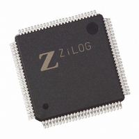
Figure 78 displays 100-pin VQFP package diagram DS007902-0708 Figure 78. 100-Pin VQFP Package Diagram Z16C30 Product Specification 96 Packaging ...
Page 101
... Ordering Information Order the Z16C30 Series from Zilog mation on ordering, consult your local Zilog sales office. The Zilog website (www.zilog.com) lists all regional offices and provides additional Z16C30 product infor- mation. Z16C30 (10 MHz) 68-Pin PLCC For fast results, contact your local Zilog desired ...
Page 102
... Customer Support For answers to technical questions about the product, documentation, or any other issues with Zilog’s offerings, please visit Zilog’s Knowledge Base at http://www.zilog.com/kb. For any comments, detail technical questions, or reporting problems, please visit Zilog’s Technical Support at http://support.zilog.com. ...