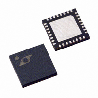
LTC1955EUH#TRPBF Linear Technology, LTC1955EUH#TRPBF Datasheet - Page 11

LTC1955EUH#TRPBF
Manufacturer Part Number
LTC1955EUH#TRPBF
Description
IC INTERFACE DL SMART CARD 32QFN
Manufacturer
Linear Technology
Datasheet
1.LTC1955EUHPBF.pdf
(20 pages)
Specifications of LTC1955EUH#TRPBF
Controller Type
Smart Card Interface
Interface
4-Wire Serial
Voltage - Supply
1.7 V ~ 5.5 V
Current - Supply
10µA
Operating Temperature
-40°C ~ 85°C
Mounting Type
Surface Mount
Package / Case
32-QFN
Lead Free Status / RoHS Status
Lead free / RoHS Compliant
Available stocks
Company
Part Number
Manufacturer
Quantity
Price
OPERATION
Table 4. Card A Communications Options
Note that if a reset is initiated with both cards selected,
then both may give an answer to reset and collide on the
DATA line. No damage will occur but data could be lost
or corrupted.
Dynamic Pull-Up Current Sources
The current sources on the bidirectional pins (DATA, I/O
A/I/O B) are dynamically activated to achieve a fast rise time
with a relatively small static current. * Once a bidirectional
pin is relinquished, a small start-up current begins to
charge the node. An edge rate detector determines if the
pin is released by comparing its slew rate with an internal
reference value. If a valid transition is detected, a large
pull-up current enhances the edge rate on the node. The
higher slew rate corroborates the decision to charge the
node thereby affecting a dynamic form of hysteresis.
Clock Channels
As described in the section Serial Port, the LTC1955 sup-
ports both synchronous and asynchronous smart cards.
On start-up, or when bits D13-D15 for card A and bits
D5-D7 for card B are set to 0s, the clock channel is in
synchronous mode. The remaining modes are used for
asynchronous cards.
In synchronous mode, the CLK A/CLK B pins follow the
SYNC pin for a channel that is selected. If a channel is
deselected (via the serial port), the CLK A/CLK B line for
that channel is latched at its current value.
D12
0
0
1
1
BIDIRECTIONAL
D11
0
1
0
1
Figure 2. Dynamic Pull-Up Current Sources
SUPPLY
LOCAL
I
START
CARD A COMMUNICATION MODE
Nothing Selected
C4A Connected to DATA Pin
C8A Connected to DATA Pin
I/O A Connected to DATA Pin
PIN
dv
dt
+
–
V
1955 F02
REF
In asynchronous mode, the CLK A/CLK B pins follow either
the ASYNC pin (÷1 mode) or a divided version of this pin.
The CLK A/CLK B pins can also be stopped high or low.
The available divider ratios include ÷2, ÷4 and ÷8. When
switching between divider ratios, the internal selection
circuitry ensures that no spikes or glitches appear on the
CLK A/CLK B pins. Consequently, it may take up to 8 clock
pulses for the clock frequency change command to take
affect. Synchronization circuitry ensures that no glitches
occur when entering or exiting one of the stop modes.
For example, when entering stop low mode, the selection
circuitry waits for the next falling edge of the respective
CLK A/CLK B signal to make the change. Likewise, if stop
high is selected, it will occur on the next rising edge.
Deselection of an asynchronous card does not affect its
CLK A/CLK B pin. Its clock can be started, stopped or its
divider ratio changed at any time.
To clean up the duty cycle of the incoming clock in asyn-
chronous applications, any of the clock divider modes ÷2,
÷4 or ÷8 will yield a very nearly 50% duty cycle.
Additional synchronization circuitry prevents glitches from
occurring when switching between synchronous mode and
asynchronous mode. Because of this circuitry, two edges
(a falling edge followed by a rising edge) are necessary
at the CLK pin to switch modes from asynchronous to
synchronous. For example, if clock stop mode is engaged,
the clock channel will not change modes until clock stop
mode is disengaged.
Any combination of cards, synchronous or asynchronous,
can be used as both channels can be set to any of the
clock modes or divider ratios independently.
Both SYNC and ASYNC inputs are independently level
shifted to the appropriate voltage for the CLK A/CLK B
pins (5V, 3V, 1.8V).
Reset Channels
When a card is selected, the reset channels provide a level
shifted path from the R
When a card is deselected, its RST A/RST B pin is latched
at the current value of R
* U.S. Patent No. 6,356,140
IN
IN
.
pin to the RST A/RST B pins.
LTC1955
11
1955fb


