TP3069N National Semiconductor, TP3069N Datasheet - Page 2
TP3069N
Manufacturer Part Number
TP3069N
Description
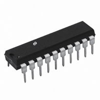
IC INTERFACE ENHANCED SER 20-DIP
Manufacturer
National Semiconductor
Series
COMBO®r
Type
PCM Codec/Filterr
Datasheet
1.TP3069N.pdf
(18 pages)
Specifications of TP3069N
Data Interface
PCM Audio Interface
Resolution (bits)
8 b
Number Of Adcs / Dacs
1 / 1
Sigma Delta
No
Voltage - Supply, Analog
4.75 V ~ 5.25 V
Voltage - Supply, Digital
4.75 V ~ 5.25 V
Operating Temperature
-25°C ~ 125°C
Mounting Type
Through Hole
Package / Case
20-DIP (0.300", 7.62mm)
Lead Free Status / RoHS Status
Contains lead / RoHS non-compliant
Other names
*TP3069N


Connection Diagrams
Pin Description
VPO
GNDA
VPO
VPI
VF
V
FS
D
BCLK
CLKSEL
MCLK
PDN
Symbol
CC
R
R
R
O
b
a
R
R
The non-inverted output of the receive power
amplifier
Analog ground All signals are referenced to
this pin
The inverted output of the receive power
amplifier
Inverting input to the receive power amplifier
Analog output of the receive filter
Positive power supply pin V
Receive frame sync pulse which enables
BCLK
8 kHz pulse train See Figures 2 and 3 for
timing details
Receive data input PCM data is shifted into
D
The bit clock which shifts data into D
the FS
to 2 048 MHz Alternatively may be a logic
input which selects either
1 536 MHz 1 544 MHz or 2 048 MHz for
master clock in synchronous mode and
BCLK
directions (see Table I)
Receive master clock Must be 1 536 MHz
1 544 MHz or 2 048 MHz May be
asynchronous with MCLK
synchronous with MCLK
performance When MCLK
continuously low MCLK
internal timing When MCLK
continuously high the device is powered
down
R
following the FS
R
X
R
is used for both transmit and receive
to shift PCM data into D
leading edge May vary from 64 kHz
Dual-In-Line Package
Top View
Function
R
leading edge
X
X
X
is selected for all
for best
R
CC
but should be
R
is connected
is connected
e a
R
FS
5V
TL H 10578–2
R
R
g
after
is an
5%
2
Symbol
MCLK
BCLK
D
FS
TS
ANLB
GS
VF
VF
V
BB
X
X
X
X
X
X
I
I
b
a
X
X
Transmit master clock Must be 1 536 MHz
1 544 MHz or 2 048 MHz May be
asynchronous with MCLK
performance is realized from synchronous
operation
The bit clock which shifts out the PCM data
on D
but must be synchronous with MCLK
The TRI-STATE PCM data output which is
enabled by FS
Transmit frame sync pulse input which
enables BCLK
D
and 3 for timing details
Open drain output which pulses low during
the encoder time slot
Analog Loopback control input Must be set
to logic ‘0’ for normal operation When pulled
to logic ‘1’ the transmit filter input is
disconnected from the output of the transmit
preamplifier and connected to the output of
the receive switched capacitor low-pass filter
and the input to the receive RC active filter is
connected to ground This results in the
VFRO output being at ground level during
analog loopback operation
Analog output of the transmit input amplifier
Used to externally set gain
Inverting input of the transmit input amplifier
Non-inverting input of the transmit input
amplifier
Negative power supply pin V
See NS Package Number N20A
See NS Package Number V20A
See NS Package Number M20B
See NS Package Number J20A
X
Order Number TP3069WM
Order Number TP3069N
FS
Order Number TP3069J
Order Number TP3069V
X
Plastic Chip Carrier
X
May vary from 64 kHz to 2 048 MHz
is an 8 kHz pulse train see Figures 2
Top View
X
X
to shift out the PCM data on
Function
R
Best
BB
eb
TL H 10578 – 3
5V
X
g
5%
Related parts for TP3069N
Image
Part Number
Description
Manufacturer
Datasheet
Request
R

Part Number:
Description:
National Semiconductor [8-Bit D/A Converter]
Manufacturer:
National Semiconductor
Datasheet:
Part Number:
Description:
National Semiconductor [Media Coprocessor]
Manufacturer:
National Semiconductor
Datasheet:
Part Number:
Description:
Digitally Controlled Tone and Volume Circuit with Stereo Audio Power Amplifier, Microphone Preamp Stage and National 3D Sound
Manufacturer:
National Semiconductor
Datasheet:
Part Number:
Description:
Digitally Controlled Tone and Volume Circuit with Stereo Audio Power Amplifier, Microphone Preamp Stage and National 3D Sound
Manufacturer:
National Semiconductor
Datasheet:
Part Number:
Description:
AC97 Rev 2 Codec with Sample Rate Conversion and National 3D Sound
Manufacturer:
National Semiconductor
Part Number:
Description:
Manufacturer:
National Semiconductor
Datasheet:
Part Number:
Description:
Manufacturer:
National Semiconductor
Datasheet:
Part Number:
Description:
General Purpose, Low Voltage, Low Power, Rail-to-Rail Output Operational Amplifiers
Manufacturer:
National Semiconductor
Datasheet:
Part Number:
Description:
8-bit 20 MSPS flash A/D converter.
Manufacturer:
National Semiconductor
Datasheet:
Part Number:
Description:
Low Noise Quad Operational Amplifier
Manufacturer:
National Semiconductor
Datasheet:
Part Number:
Description:
Quad Differential Line Receivers
Manufacturer:
National Semiconductor
Datasheet:
Part Number:
Description:
Quad High Speed Trapezoidal? Bus Transceiver
Manufacturer:
National Semiconductor
Datasheet:
Part Number:
Description:
Dual Line Receiver
Manufacturer:
National Semiconductor
Datasheet:
Part Number:
Description:
TTL to 10k ECL Level Translator with Latch
Manufacturer:
National Semiconductor
Datasheet: