TP3054N/NOPB National Semiconductor, TP3054N/NOPB Datasheet - Page 5
TP3054N/NOPB
Manufacturer Part Number
TP3054N/NOPB
Description
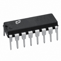
IC FILTER ENHANCE INTERFAC 16DIP
Manufacturer
National Semiconductor
Series
COMBO®r
Type
PCM Codec/Filterr
Datasheet
1.TP3054WMXNOPB.pdf
(16 pages)
Specifications of TP3054N/NOPB
Data Interface
Serial
Number Of Adcs / Dacs
1 / 1
Sigma Delta
No
Voltage - Supply, Analog
±5V
Voltage - Supply, Digital
±5V
Operating Temperature
-25°C ~ 125°C
Mounting Type
Through Hole
Package / Case
16-DIP (0.300", 7.62mm)
Lead Free Status / RoHS Status
Lead free / RoHS Compliant
Other names
*TP3054N
*TP3054N/NOPB
TP3054N
*TP3054N/NOPB
TP3054N


DIGITAL INTERFACE
V
V
V
V
I
I
I
ANALOG INTERFACE WITH TRANSMIT INPUT AMPLIFIER (ALL DEVICES)
I
R
R
R
C
V
A
F
V
V
CMRRXA
PSRRXA
ANALOG INTERFACE WITH RECEIVE FILTER (ALL DEVICES)
R
R
C
VOS
POWER DISSIPATION (ALL DEVICES)
I
I
I
I
IL
IH
OZ
I
CC
BB
CC
BB
Symbol
Absolute Maximum Ratings
If Military Aerospace specified devices are required
please contact the National Semiconductor Sales
Office Distributors for availability and specifications
V
V
Voltage at any Analog Input
Electrical Characteristics
are assured by correlation with other production tests and or product design and characterization All signals referenced to
GNDA Typicals specified at V
Note I
e
XA
IL
IH
OL
OH
O
U
OS
CM
I
O
L
L
V
O
L
L
XA
CC
BB
XA
XA
RF
RF
XA
XA
XA
or Output
XA
RF
0
1
0
1
5 0V
XA
XA
R
to GNDA
to GNDA
O
CC0
g
and I
5% V
Input Low Voltage
Input High Voltage
Output Low Voltage
Output High Voltage
Input Low Current
Input High Current
Output Current in High Impedance
State (TRI-STATE)
Input Leakage Current
Input Resistance
Output Resistance
Load Resistance
Load Capacitance
Output Dynamic Range
Voltage Gain
Unity Gain Bandwidth
Offset Voltage
Common-Mode Voltage
Common-Mode Rejection Ratio
Power Supply Rejection Ratio
Output Resistance
Load Resistance
Load Capacitance
Output DC Offset Voltage
Power-Down Current
Power-Down Current
Power-Up Active Current
Power-Up Active Current
BB0
BB
are measured after first achieving a power-up state
e b
Parameter
5 0V
g
CC
5% T
e
V
CC
5 0V V
A
a
e
0 3V to V
0 C to 70 C by correlation with 100% electrical testing at T
Unless otherwise noted limits printed in BOLD characters are guaranteed for V
BB
e b
BB
D
SIG
TS
D
SIG
GNDA
V
D
b
b
Closed Loop Unity Gain
GS
GS
GS
VF
CMRRXA
DC Test
DC Test
Pin VF
VF
No Load (Note)
No Load (Note)
No Load
No Load
IH s
b
5 0V T
X
X
X
2 5V
2 5V
X
X
R
X
X
X
b
0 3V
R
R
I
I
GNDA
I
O
L
H
a
I
V
7V
7V
R
e
L
eb
e
I
I
s
R
s
s
L
e
H
IN s
L t
to GS
O
3 2 mA
e
eb
g
V
A
V
V
3 2 mA Open Drain
IN s
1 0 mA
s
s
10 k
l
3 2 mA
s
2 5V
V
e
5
CC
Conditions
V
a
a
60 dB
1 0 mA
X
25 C
V
O s
2 5V VF
2 5V VF
IL
Voltage at any Digital Input or
Operating Temperature Range
Storage Temperature Range
Lead Temperature (Soldering 10 seconds)
ESD (Human Body Model)
Latch-Up Immunity
V
Output
All Digital Inputs
CC
X
X
I
I
a
a
or VF
or VF
X
X
I
I
b
b
e
100 mA on any Pin
b
b
5000
b
b
b
b
b
b
Min
2 2
2 4
2 4
600
60
60
200
200
10
10
2 8
1
10
10
10
20
2 5
V
CC
A
a
e
0 05
Typ
0 5
5 0
5 0
1
2
1
0 3V to GNDA
25 C All other limits
b
b
25 C to
65 C to
200
200
Max
0 6
0 4
0 4
0 4
2 8
1 5
0 3
9 0
9 0
500
10
10
10
20
2 5
50
3
3
a
a
b
2000V
125 C
150 C
300 C
Units
0 3V
MHz
V V
M
mV
mV
mA
mA
mA
mA
k
nA
pF
dB
dB
pF
CC
V
V
V
V
V
V
V
V
V
A
A
A
Related parts for TP3054N/NOPB
Image
Part Number
Description
Manufacturer
Datasheet
Request
R

Part Number:
Description:
Serial Interface CODEC IC
Manufacturer:
National Semiconductor
Datasheet:

Part Number:
Description:
IC ENHANCED INTERFACE SER 16-DIP
Manufacturer:
National Semiconductor
Datasheet:
Part Number:
Description:
National Semiconductor [8-Bit D/A Converter]
Manufacturer:
National Semiconductor
Datasheet:
Part Number:
Description:
National Semiconductor [Media Coprocessor]
Manufacturer:
National Semiconductor
Datasheet:
Part Number:
Description:
Digitally Controlled Tone and Volume Circuit with Stereo Audio Power Amplifier, Microphone Preamp Stage and National 3D Sound
Manufacturer:
National Semiconductor
Datasheet:
Part Number:
Description:
Digitally Controlled Tone and Volume Circuit with Stereo Audio Power Amplifier, Microphone Preamp Stage and National 3D Sound
Manufacturer:
National Semiconductor
Datasheet:
Part Number:
Description:
AC97 Rev 2 Codec with Sample Rate Conversion and National 3D Sound
Manufacturer:
National Semiconductor
Part Number:
Description:
Manufacturer:
National Semiconductor
Datasheet:
Part Number:
Description:
Manufacturer:
National Semiconductor
Datasheet:
Part Number:
Description:
General Purpose, Low Voltage, Low Power, Rail-to-Rail Output Operational Amplifiers
Manufacturer:
National Semiconductor
Datasheet:
Part Number:
Description:
8-bit 20 MSPS flash A/D converter.
Manufacturer:
National Semiconductor
Datasheet:
Part Number:
Description:
Low Noise Quad Operational Amplifier
Manufacturer:
National Semiconductor
Datasheet:
Part Number:
Description:
Quad Differential Line Receivers
Manufacturer:
National Semiconductor
Datasheet:
Part Number:
Description:
Quad High Speed Trapezoidal? Bus Transceiver
Manufacturer:
National Semiconductor
Datasheet: