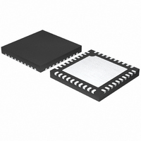
MAX9856ETL+ Maxim Integrated Products, MAX9856ETL+ Datasheet - Page 26

MAX9856ETL+
Manufacturer Part Number
MAX9856ETL+
Description
IC CODEC AUDIO LP 40TQFN-EP
Manufacturer
Maxim Integrated Products
Type
Audio Codecr
Datasheet
1.MAX9856ETL.pdf
(46 pages)
Specifications of MAX9856ETL+
Data Interface
Serial
Resolution (bits)
18 b
Number Of Adcs / Dacs
2 / 2
Sigma Delta
Yes
S/n Ratio, Adcs / Dacs (db) Typ
77 / 91
Dynamic Range, Adcs / Dacs (db) Typ
85 / 91
Voltage - Supply, Analog
1.71 V ~ 3.6 V
Voltage - Supply, Digital
1.71 V ~ 3.6 V
Operating Temperature
-40°C ~ 85°C
Mounting Type
Surface Mount
Package / Case
40-WFQFN Exposed Pad
Number Of Adc Inputs
2
Number Of Dac Outputs
2
Interface Type
I2C
Resolution
18 bit
Operating Supply Voltage
1.71 V to 3.6 V
Maximum Operating Temperature
+ 85 C
Mounting Style
SMD/SMT
Minimum Operating Temperature
- 40 C
Supply Current
2.9 mA
Thd Plus Noise
82 dB
Audio Codec Type
Stereo
No. Of Adcs
2
No. Of Dacs
2
No. Of Input Channels
2
No. Of Output Channels
2
Adc / Dac Resolution
18bit
Adcs / Dacs Signal To Noise Ratio
91dB
Rohs Compliant
Yes
Lead Free Status / RoHS Status
Lead free / RoHS Compliant
Low-Power Audio CODEC with
DirectDrive Headphone Amplifiers
ADC Interface Register Bit Description (continued)
26
______________________________________________________________________________________
REGISTER
APLLEN
ADCNI
AGAIN
ADLY
APIN
LRCLK_A/GPIO Configuration:
00 = General-purpose input
01 = Word clock for the ADC
10 = General-purpose output—low
11 = General-purpose output—high
When APIN ≠ 01, LRCLK_D is used as the word clock for both the DAC and ADC. AWCI, ABCI, and
ADLY are still active and independent from the DAC mode bit settings when operating with a shared
LRCLK_D.
ADC Data Delay
0—The most significant bit of an audio word is valid at the first BCLK edge after the LRCLK_A
transition.
1—The most significant bit of an audio word is valid at the second BCLK edge after the LRCLK_A
transition.
(ADLY = 1 for I
ADC PLL Enable. This bit only applies when APIN = 01. When APIN ≠ 01 use DPLLEN for both the
DAC and ADC:
0 (Valid for slave and master mode)—The frequency of LRCLK_A is set by the ADCNI divider bits. In
master mode, the MAX9856 generates LRCLK_A using the specified divide ratio. In slave mode, the
MAX9856 expects an LRCLK_A using specified divide ratio.
1 (Valid for slave mode only)—A digital PLL locks on to any externally supplied LRCLK_A signal
regardless of the MCLK frequency.
ADC LRCLK Divider. If APIN ≠ 01, use DACNI for both the DAC and ADC. When APLLEN is set low,
the frequency of LRCLK_A is determined by ADCNI. See Table 6 for common ADCNI values:
ADCNI = (65536 x 96 x f
f
f
ADC Output Gain. Specifies the gain applied to the digital output of the ADC prior to being output
from the device.
LRCLK_A
PCLK
= Prescaled MCLK internal clock frequency (PCLK).
= LRCLK_A frequency.
2
S-compatible mode)
VALUE
LRCLK_A
0xA
0xB
0xC
0xD
0x0
0x1
0x2
0x3
0x4
0x5
0x6
0x7
0x8
0x9
0xE
0xF
)/f
PCLK
.
FUNCTION
GAIN (dB)
-10
-11
-12
+3
+2
+1
-1
-2
-3
-4
-5
-6
-7
-8
-9
0


