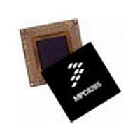
MPC8250ACVVMHBC Freescale Semiconductor, MPC8250ACVVMHBC Datasheet - Page 59

MPC8250ACVVMHBC
Manufacturer Part Number
MPC8250ACVVMHBC
Description
IC MPU POWERQUICC II 480-TBGA
Manufacturer
Freescale Semiconductor
Datasheet
1.MPC8250AVRIHBC.pdf
(62 pages)
Specifications of MPC8250ACVVMHBC
Processor Type
MPC82xx PowerQUICC II 32-bit
Speed
266MHz
Voltage
2V
Mounting Type
Surface Mount
Package / Case
480-TBGA
Family Name
MPC82XX
Device Core
PowerQUICC II
Device Core Size
32b
Frequency (max)
266MHz
Instruction Set Architecture
RISC
Operating Supply Voltage (max)
2.2V
Operating Supply Voltage (min)
1.9V
Operating Temp Range
-40C to 105C
Operating Temperature Classification
Industrial
Mounting
Surface Mount
Pin Count
480
Package Type
TBGA
Leaded Process Compatible
Yes
Rohs Compliant
Yes
Peak Reflow Compatible (260 C)
Yes
For Use With
CWH-PPC-8248N-VE - KIT EVAL SYSTEM QUICCSTART 8248
Lead Free Status / RoHS Status
Lead free / RoHS Compliant
Features
-
Lead Free Status / Rohs Status
Compliant
Available stocks
Company
Part Number
Manufacturer
Quantity
Price
Company:
Part Number:
MPC8250ACVVMHBC
Manufacturer:
FREESCAL
Quantity:
390
Company:
Part Number:
MPC8250ACVVMHBC
Manufacturer:
Freescale Semiconductor
Quantity:
10 000
Part Number:
MPC8250ACVVMHBC
Manufacturer:
FREESCALE
Quantity:
20 000
6
Figure 19
addition to the processor frequency, the part numbering scheme also consists of a part modifier that
indicates any enhancement(s) in the part from the original production design. Each part number also
contains a revision code that refers to the die mask revision number and is specified in the part numbering
scheme for identification purposes only. For more information, contact your local Freescale sales office.
7
Table 24
Freescale Semiconductor
Revision
Product Code
Device Number
Process Technology
(A = 0.25 micron)
Temperature Range
(Blank = 0 to 105 °C
0.9
0.8
0.7
Ordering Information
Document Revision History
2
1
C = –40 to 105 °C)
provides a revision history for this template.
provides an example of the Freescale part numbering nomenclature for the MPC8250. In
11/2002
10/2002
7/2009
3/2005
8/2003
Date
Updated TBGA and PBGA packaging information.
Document template update
Table
Table
•
• Addition of VCCSYN to “Note: Core, PLL, and I/O Supply Voltages” following
• Addition of
• Addition of note 1 to
•
•
•
•
•
•
• Addition of SPICLK to PC19 in
MPC 8250 A C
Table
Table
Table
Figure 3
Table
Table
Table 20
MPC8260 PowerQUICC II™ Family Reference Manual but had previously been omitted from
Table 20
22, “VR Pinout”: Addition of C18 to the Ground (GND) pin list (page 53)
22, “VR Pinout”: Addition of L3 to the Core (VDDx) pin list (page 53)
2: Modification to supply voltage ranges reflected in notes 2, 3, and 4
4: Changes to θ
7,
9: Change to sp10
14,
Figure
through
and
and
Table
Figure 2
Figure 19. Freescale Part Number Key
MPC8250 Hardware Specifications, Rev. 2
Table 24. Document Revision History
Table
Table
8: Addition of sp42a/sp43a
16, and
Figure
22: Addition of note 1
22.
Table 3
JA
. Addition of θ
Table
8: Addition of notes or modifications
18: Removal of PLL bypass mode from clock tables
Table 20
ZU XXX
Substantive Changes
JB
and θ
and
Table
JC
22. It is documented correctly in the
X
ZU = 480 TBGA
VV = 480 TBGA (Pb free)
ZO = 516 PBGA
VR = 516 PBGA (Pb free)
Processor Frequency
Die Revision Level
(CPU/CPM/Bus)
Table 2
Ordering Information
Package
59


