IS80C286-20 Intersil, IS80C286-20 Datasheet - Page 28
IS80C286-20
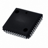
Manufacturer Part Number
IS80C286-20
Description
IC CPU 16BIT 5V 20MHZ 68-PLCC
Manufacturer
Intersil
Datasheet
1.CS80C286-12.pdf
(60 pages)
Specifications of IS80C286-20
Processor Type
80C286 16-Bit
Speed
20MHz
Voltage
5V
Mounting Type
Surface Mount
Package / Case
68-PLCC
Lead Free Status / RoHS Status
Contains lead / RoHS non-compliant
Features
-
Available stocks
Company
Part Number
Manufacturer
Quantity
Price


Bus States
The idle (T
progress or requested. The first active state T
by status line S1 or S0 going LOW and identifying phase 1 of
the processor clock. During T
address, and data (for a write operation) are available on the
80C286 output pins. The 82C288 bus controller decodes the
status signals and generates Multibus compatible read/write
command and local transceiver control signals.
After T
ory or I/O devices respond to the bus operation during T
either transferring read data to the CPU or accepting write
data. T
ensure sufficient time for the memory or I/O device to
respond. The READY signal determines whether T
repeated. A repeated T
During hold (T
status output drivers enabling another bus master to use the
local bus. The 80C286 HOLD input signal is used to place
the 80C286 into the T
nal indicates that the CPU has entered T
Pipelined Addressing
The 80C286 uses a local bus interface with pipelined timing
to allow as much time as possible for data access. Pipelined
timing allows a new bus operation to be initiated every two
processor cycles, while allowing each individual bus opera-
tion to last for three processor cycles.
The timing of the address outputs is pipelined such that the
address of the next bus operation becomes available during
the current bus operation. Or, in other words, the first clock of
the next bus operation is overlapped with the last clock of the
current bus operation. Therefore, address decode and routing
logic can operate in advance of the next bus operation.
External address latches may hold the address stable for the
entire bus operation, and provide additional AC and DC buff-
ering.
The 80C286 does not maintain the address of the current bus
operation during all T
next bus operation may be emitted during phase 2 of any T
HLDA • NEW CYCLE
HLDA
HOLD
S
C
T
, the perform command (T
H
states may be repeated as often as necessary to
I
) state indicates that no data transfers are in
HLDA • NEW CYCLE
FIGURE 21. 80C286 BUS STATES
H
), the 80C286 will float all address, data, and
HLDA
STATUS
H
T
C
S
C
state. The 80C286 HLDA output sig-
RESET
states. Instead, the address for the
READY • NEW CYCLE
state is called a wait state.
NEW CYCLE
S
ALWAYS
, the command encoding, the
IDLE
T
C
I
) state is entered. Mem-
H
COMMAND
READY • NEW CYCLE
NEW CYCLE • HLDA
.
T
C
S
is signaled
READY
C
80C286
C
C
is
,
.
28
The address remains valid during phase 1 of the first T
guarantee hold time, relative to ALE, for the address latch
inputs.
Bus Control Signals
The 82C288 bus controller provides control signals; address
latch enable (ALE), Read/Write commands, data trans-
mit/receive (DT/R), and data enable (DEN) that control the
address latches, data transceivers, write enable, and output
enable for memory and I/O systems.
The Address Latch Enable (ALE) output determines when
the address may be latched. ALE provides at least one sys-
tem CLK period of address hold time from the end of the pre-
vious bus operation until the address for the next bus
operation appears at the latch outputs. This address hold
time is required to support Multibus and common memory
systems.
The data bus transceivers are controlled by 82C288 outputs
Data Enable (DEN) and Data Transmit/Receive (DT/R). DEN
enables the data transceivers; while DT/R controls trans-
ceiver direction. DEN and DT/R are timed to prevent bus
contention between the bus master, data bus transceivers,
and system data bus transceivers.
Command Timing Controls
Two system timing customization options, command extension
and command delay, are provided on the 80C286 local bus.
Command extension allows additional time for external
devices to respond to a command and is analogous to
inserting wait states on the 80C86. External logic can control
the duration of any bus operation such that the operation is
only as long as necessary. The READY input signal can
extend any bus operation for as long as necessary.
Command delay allows an increase of address or write data
setup time to system bus command active for any bus oper-
ation by delaying when the system bus command becomes
active. Command delay is controlled by the 82C288 CMDLY
input. After T
failing edge of CLK. If CMDLY is HIGH, the 82C288 will not
activate the command signal. When CMDLY is LOW, the
82C288 will activate the command signal. After the com-
mand becomes active, the CMDLY input is not sampled.
When a command is delayed, the available response time
from command active to return read data or accept write
data is less. To customize system bus timing, an address
decoder can determine which bus operations require delay-
ing the command. The CMDLY input does not affect the tim-
ing of ALE, DEN or DT/R.
Figure 23 illustrates four uses of CMDLY. Example 1 shows
delaying the read command two system CLKs for cycle N-1
and no delay for cycle N, and example 2 shows delaying the
read command one system CLK for cycle N-1 and one sys-
tem CLK delay for cycle N.
S
, the bus controller samples CMDLY at each
C
to
Related parts for IS80C286-20
Image
Part Number
Description
Manufacturer
Datasheet
Request
R

Part Number:
Description:
Intersil Corporation [CMOS Serial Controller Interface]
Manufacturer:
Intersil Corporation
Datasheet:
Part Number:
Description:
Manufacturer:
Intersil Corporation
Datasheet:
Part Number:
Description:
357-036-542-201 CARDEDGE 36POS DL .156 BLK LOPRO
Manufacturer:
Intersil Corporation
Datasheet:
Part Number:
Description:
1024-Word x 4-Bit LSI Static RAM
Manufacturer:
Intersil Corporation
Datasheet:
Part Number:
Description:
General Purpose NPN Transistor Arrays FN341.4
Manufacturer:
Intersil Corporation
Datasheet:
Part Number:
Description:
CMOS 16-Bit Microprocessor
Manufacturer:
Intersil Corporation
Datasheet:
Part Number:
Description:
Manufacturer:
Intersil Corporation
Datasheet:
Part Number:
Description:
Manufacturer:
Intersil Corporation
Datasheet:
Part Number:
Description:
Manufacturer:
Intersil Corporation
Datasheet:
Part Number:
Description:
Manufacturer:
Intersil Corporation
Datasheet:
Part Number:
Description:
CMOS 6-Bit Latch and Decoder Memory Interfaces
Manufacturer:
Intersil Corporation
Datasheet:
Part Number:
Description:
CA3046General Purpose NPN Transistor Arrays
Manufacturer:
Intersil Corporation
Datasheet:
Part Number:
Description:
Manufacturer:
Intersil Corporation
Datasheet:
Part Number:
Description:
TR909 DLC/FLC SLIC with Low Power Standby
Manufacturer:
Intersil Corporation
Datasheet:
Part Number:
Description:
Manufacturer:
Intersil Corporation
Datasheet: