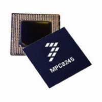
MPC8245TVV300D Freescale Semiconductor, MPC8245TVV300D Datasheet - Page 38

MPC8245TVV300D
Manufacturer Part Number
MPC8245TVV300D
Description
IC MPU 32BIT 300MHZ PPC 352-TBGA
Manufacturer
Freescale Semiconductor
Datasheet
1.MPC8245LZU266D.pdf
(68 pages)
Specifications of MPC8245TVV300D
Processor Type
MPC82xx PowerQUICC II 32-bit
Speed
300MHz
Voltage
1.8V
Mounting Type
Surface Mount
Package / Case
352-TBGA
Processor Series
MPC8xxx
Core
603e
Data Bus Width
32 bit
Maximum Clock Frequency
300 MHz
Operating Supply Voltage
1.8 V, 1.9 V, 2 V, 3.3 V
Maximum Operating Temperature
+ 105 C
Mounting Style
SMD/SMT
Minimum Operating Temperature
- 40 C
Lead Free Status / RoHS Status
Lead free / RoHS Compliant
Features
-
Lead Free Status / Rohs Status
Lead free / RoHS Compliant
Available stocks
Company
Part Number
Manufacturer
Quantity
Price
Company:
Part Number:
MPC8245TVV300D
Manufacturer:
Freescale Semiconductor
Quantity:
135
Company:
Part Number:
MPC8245TVV300D
Manufacturer:
Freescale Semiconductor
Quantity:
10 000
Part Number:
MPC8245TVV300D
Manufacturer:
FREESCALE
Quantity:
20 000
Package Description
38
DA[14:15]
Notes:
1. Place a pull-up resistor of 120 Ω or less on the TEST0 pin.
2. Treat these pins as no connects (NC) unless debug address functionality is used.
3. This pin has an internal pull-up resistor that is enabled only in the reset state. The value of the internal pull-up resistor is not
4. This pin is a reset configuration pin.
5. DL[0] is a reset configuration pin with an internal pull-up resistor that is enabled only in the reset state. The value of the
6. Multi-pin signals such as AD[31:0] and MDL[0:31] have their physical package pin numbers listed in an order corresponding
7. GNT4 is a reset configuration pin with an internal pull-up resistor that is enabled only in the reset state.
8. A weak pull-up resistor (2–10 kΩ) should be placed on this PCI control pin to LV
9. V
10. A weak pull-up resistor (2–10 kΩ) should be placed on this pin to OV
11. A weak pull-up resistor (2–10 kΩ) should be placed on this pin to GV
12. This pin has an internal pull-up resistor that is enabled at all times. The value of the internal pull-up resistor is not guaranteed
13. An external PCI clocking source or fan-out buffer may be required for the MPC8245 DUART functionality since
14. This pin is a multiplexed signal and appears more than once in this table.
15. This pin is affected by the programmable PCI_HOLD_DEL parameter.
16. This pin is an open-drain signal.
17. This pin can be programmed as driven (default) or as open-drain (in MIOCR 1).
18. This pin is a sustained three-state pin as defined by the PCI Local Bus Specification.
19. OSC_IN uses the 3.3-V PCI interface driver, which is 5-V tolerant. See
20. PLL_CFG signals must be driven on reset and must be held for at least 25 clock cycles after the negation of HRST_CTRL
21. SDRAM_CLK[0:3] and SDRAM_SYNC_OUT signals use DRV_MEM_CTRL for chip Rev 1.1 (A). These signals use
22. The 266- and 300-MHz part offerings can run at a source voltage of 1.8 ± 100 mV or 2.0 ± 100 mV. Source voltage should
23. This pin is LAVDD on the MPC8240. It is an NC on the MPC8245, which should not pose a problem when an MPC8240 is
24. The driver capability of this pin is hardwired to 40 Ω and cannot be changed.
25. A weak pull-up resistor (2–10 kΩ) should be placed on this pin to OV
26. Typically, the serial port has sufficient drivers in the RS232 transceiver to drive the CTS pin actively as an input. No pullups
27. HRST_CPU/HRST_CTRL must transition from a logic 0 to a logic 1 in less than one SDRAM_SYNC_IN clock cycle for the
guaranteed but is sufficient to ensure that a logic 1 is read into configuration bits during reset if the signal is left unterminated.
internal pull-up resistor is not guaranteed but is sufficient to ensure that a logic 1 is read into configuration bits during reset.
to the signal names. Example: AD0 is on pin C22, AD1 is on pin D22, ..., AD31 is on pin V25.
but is sufficient to prevent unused inputs from floating.
PCI_CLK[0:3] are not available in DUART mode. Only PCI_CLK4 is available in DUART mode.
and HRST_CPU in order to be latched.
DRV_MEM_CLK for chip Rev 1.2 (B).
be 2.0 ± 100 mV for 333- and 350-MHz parts.
replaced with an MPC8245.
memory clock is not used and PLL[0:4] does not select a half-clock frequency ratio.
are needed in this case.
device to be in the nonreset state
IH
and V
Name
IL
for these signals are the same as the PCI V
F1 J2
MPC8245 Integrated Processor Hardware Specifications, Rev. 10
Pin Numbers
Table 16. MPC8245 Pinout Listing (continued)
IH
and V
Output
Type
IL
entries in
DD
DD
DD
Table 2
.
.
so that a 1 can be detected at reset if an external
Supply
Power
Table
GV
for details.
DD
DD
3.
.
DRV_MEM_CTRL
Driver Type
Output
Freescale Semiconductor
Notes
2, 6


