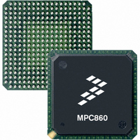
MPC855TZQ66D4 Freescale Semiconductor, MPC855TZQ66D4 Datasheet - Page 3

MPC855TZQ66D4
Manufacturer Part Number
MPC855TZQ66D4
Description
IC MPU PWRQUICC 50MHZ 357-PBGA
Manufacturer
Freescale Semiconductor
Series
PowerQUICCr
Specifications of MPC855TZQ66D4
Processor Type
MPC8xx PowerQUICC 32-Bit
Speed
66MHz
Voltage
3.3V
Mounting Type
Surface Mount
Package / Case
357-PBGA
Processor Series
MPC8xx
Core
MPC8xx
Data Bus Width
32 bit
Maximum Clock Frequency
66 MHz
Operating Supply Voltage
2.5 V, 3.3 V
Maximum Operating Temperature
+ 105 C
Mounting Style
SMD/SMT
Data Ram Size
4 KB
I/o Voltage
3.3 V
Interface Type
I2C, SPI, UART
Minimum Operating Temperature
0 C
Family Name
MPC8xx
Device Core
PowerQUICC
Device Core Size
32b
Frequency (max)
66MHz
Instruction Set Architecture
RISC
Supply Voltage 1 (typ)
2.5/3.3V
Operating Supply Voltage (max)
3.465/3.6V
Operating Supply Voltage (min)
2/3.135V
Operating Temp Range
0C to 95C
Operating Temperature Classification
Commercial
Mounting
Surface Mount
Pin Count
357
Package Type
BGA
Core Size
32 Bit
Program Memory Size
8KB
Cpu Speed
66MHz
Digital Ic Case Style
BGA
No. Of Pins
357
Supply Voltage Range
2V To 3.6V
Operating Temperature Range
0°C To +95°C
Rohs Compliant
No
Lead Free Status / RoHS Status
Contains lead / RoHS non-compliant
Features
-
Lead Free Status / Rohs Status
Lead free / RoHS Compliant
Available stocks
Company
Part Number
Manufacturer
Quantity
Price
Company:
Part Number:
MPC855TZQ66D4
Manufacturer:
Freescale Semiconductor
Quantity:
10 000
Part Number:
MPC855TZQ66D4
Manufacturer:
N/A
Quantity:
20 000
2
The following list summarizes the key MPC860 features:
Freescale Semiconductor
•
•
•
•
•
•
Features
Embedded single-issue, 32-bit core (implementing the Power Architecture technology) with
thirty-two 32-bit general-purpose registers (GPRs)
— The core performs branch prediction with conditional prefetch without conditional execution.
— 4- or 8-Kbyte data cache and 4- or 16-Kbyte instruction cache (see
— MMUs with 32-entry TLB, fully-associative instruction, and data TLBs
— MMUs support multiple page sizes of 4-, 16-, and 512-Kbytes, and 8-Mbytes; 16 virtual
— Advanced on-chip-emulation debug mode
Up to 32-bit data bus (dynamic bus sizing for 8, 16, and 32 bits)
32 address lines
Operates at up to 80 MHz
Memory controller (eight banks)
— Contains complete dynamic RAM (DRAM) controller
— Each bank can be a chip select or RAS to support a DRAM bank.
— Up to 15 wait states programmable per memory bank
— Glueless interface to DRAM, SIMMS, SRAM, EPROM, Flash EPROM, and other memory
— DRAM controller programmable to support most size and speed memory interfaces
— Four CAS lines, four WE lines, and one OE line
— Boot chip-select available at reset (options for 8-, 16-, or 32-bit memory)
— Variable block sizes (32 Kbytes to 256 Mbytes)
— Selectable write protection
— On-chip bus arbitration logic
General-purpose timers
— Four 16-bit timers or two 32-bit timers
— Gate mode can enable/disable counting
— Interrupt can be masked on reference match and event capture.
– 16-Kbyte instruction caches are four-way, set-associative with 256 sets; 4-Kbyte instruction
– 8-Kbyte data caches are two-way, set-associative with 256 sets; 4-Kbyte data caches are
– Cache coherency for both instruction and data caches is maintained on 128-bit (4-word)
– Caches are physically addressed, implement a least recently used (LRU) replacement
address spaces and 16 protection groups
devices
caches are two-way, set-associative with 128 sets.
two-way, set-associative with 128 sets.
cache blocks.
algorithm, and are lockable on a cache block basis.
MPC860 PowerQUICC™ Family Hardware Specifications, Rev. 8
Table
1)
Features
3


