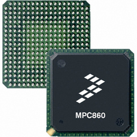
MPC885CZP66 Freescale Semiconductor, MPC885CZP66 Datasheet - Page 23

MPC885CZP66
Manufacturer Part Number
MPC885CZP66
Description
IC MPU POWERQUICC 66MHZ 357PBGA
Manufacturer
Freescale Semiconductor
Datasheet
1.MPC880VR80.pdf
(87 pages)
Specifications of MPC885CZP66
Processor Type
MPC8xx PowerQUICC 32-Bit
Speed
66MHz
Voltage
3.3V
Mounting Type
Surface Mount
Package / Case
357-PBGA
For Use With
CWH-PPC-885XN-VX - BOARD EVAL QUICCSTART MPC885CWH-PPC-885XN-VE - BOARD EVAL QUICCSTART MPC885
Lead Free Status / RoHS Status
Contains lead / RoHS non-compliant
Features
-
Available stocks
Company
Part Number
Manufacturer
Quantity
Price
Company:
Part Number:
MPC885CZP66
Manufacturer:
TI/NSC
Quantity:
769
Company:
Part Number:
MPC885CZP66
Manufacturer:
Freescale Semiconductor
Quantity:
10 000
1
2
3
4
5
6
7
8
9
10
Freescale Semiconductor
For part speeds above 50 MHz, use 9.80 ns for B11a.
The timing required for BR input is relevant when the MPC885/MPC880 is selected to work with the internal bus arbiter. The
timing for BG input is relevant when the MPC885/MPC880 is selected to work with the external bus arbiter.
For part speeds above 50 MHz, use 2 ns for B17.
The D(0:31) input timings B18 and B19 refer to the rising edge of the CLKOUT in which the TA input signal is asserted.
For part speeds above 50 MHz, use 2 ns for B19.
The D(0:31) input timings B20 and B21 refer to the falling edge of the CLKOUT. This timing is valid only for read accesses
controlled by chip-selects under control of the user-programmable machine (UPM) in the memory controller, for data beats
where DLT3 = 1 in the RAM words. (This is only the case where data is latched on the falling edge of CLKOUT.)
This formula applies to bus operation up to 50 MHz.
The timing B30 refers to CS when ACS = 00 and to CS and WE(0:3) when CSNT = 0.
The signal UPWAIT is considered asynchronous to the CLKOUT and synchronized internally. The timings specified in B37 and
B38 are specified to enable the freeze of the UPM output signals as described in
The AS signal is considered asynchronous to the CLKOUT. The timing B39 is specified in order to allow the behavior specified
in
Num
B36
B37
B38
B39
B40
B41
B42
B43
Figure
A(0:31), BADDR(28:30), and D(0:31) to GPL
valid, as requested by control bit GxT4 in the
corresponding word in the UPM
(MIN = 0.25 × B1 – 2.00)
UPWAIT valid to CLKOUT falling edge
(MIN = 0.00 × B1 + 6.00)
CLKOUT falling edge to UPWAIT valid
(MIN = 0.00 × B1 + 1.00)
AS valid to CLKOUT rising edge
(MIN = 0.00 × B1 + 7.00)
A(0:31), TSIZ(0:1), RD/WR, BURST, valid to
CLKOUT rising edge (MIN = 0.00 × B1 + 7.00)
TS valid to CLKOUT rising edge (setup time)
(MIN = 0.00 × B1 + 7.00)
CLKOUT rising edge to TS valid (hold time)
(MIN = 0.00 × B1 + 2.00)
AS negation to memory controller signals
negation (MAX = TBD)
24.
Characteristic
MPC885/MPC880 PowerQUICC Hardware Specifications, Rev. 7
Table 9. Bus Operation Timings (continued)
10
9
9
5.60
6.00
1.00
7.00
7.00
7.00
2.00
Min
—
33 MHz
Max
TBD
—
—
—
—
—
—
—
4.30
6.00
1.00
7.00
7.00
7.00
2.00
Min
—
40 MHz
Figure
Max
TBD
—
—
—
—
—
—
—
21.
1.80
6.00
1.00
7.00
7.00
7.00
2.00
Min
—
66 MHz
Max
TBD
—
—
—
—
—
—
—
1.13
6.00
1.00
7.00
7.00
7.00
2.00
Min
—
80 MHz
Bus Signal Timing
TBD
Max
—
—
—
—
—
—
—
Unit
ns
ns
ns
ns
ns
ns
ns
ns
23


