MPC8323CVRADDC Freescale Semiconductor, MPC8323CVRADDC Datasheet - Page 65
MPC8323CVRADDC
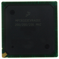
Manufacturer Part Number
MPC8323CVRADDC
Description
IC MPU PWRQUICC II 516-PBGA
Manufacturer
Freescale Semiconductor
Datasheet
1.MPC8321VRADDC.pdf
(82 pages)
Specifications of MPC8323CVRADDC
Processor Type
MPC83xx PowerQUICC II Pro 32-Bit
Speed
266MHz
Voltage
1V
Mounting Type
Surface Mount
Package / Case
516-PBGA
For Use With
MPC8323E-RDB - BOARD REFERENCE DESIGN
Lead Free Status / RoHS Status
Lead free / RoHS Compliant
Features
-
Available stocks
Company
Part Number
Manufacturer
Quantity
Price
Company:

Part Number:
MPC8323CVRADDC
Manufacturer:
Freescale Semiconductor
Quantity:
10 000


22.1
When the MPC8323E is configured as a PCI host device (RCWH[PCIHOST] = 1), CLKIN is its primary
input clock. CLKIN feeds the PCI clock divider (÷2) and the PCI_SYNC_OUT and PCI_CLK_OUT
multiplexors. The CFG_CLKIN_DIV configuration input selects whether CLKIN or CLKIN/2 is driven
out on the PCI_SYNC_OUT signal.
PCI_SYNC_OUT is connected externally to PCI_SYNC_IN to allow the internal clock subsystem to
synchronize to the system PCI clocks. PCI_SYNC_OUT must be connected properly to PCI_SYNC_IN,
with equal delay to all PCI agent devices in the system.
22.1.1
When the MPC8323E is configured as a PCI host, it provides three separate clock output signals,
PCI_CLK_OUT[0:2], for external PCI agents.
When the device comes out of reset, the PCI clock outputs are disabled and are actively driven to a steady
low state. Each of the individual clock outputs can be enabled (enable toggling of the clock) by setting its
corresponding OCCR[PCICOEn] bit. All output clocks are phase-aligned to each other.
22.2
When the MPC8323E is configured as a PCI agent device, PCI_CLK is the primary input clock. In agent
mode, the CLKIN signal should be tied to GND, and the clock output signals, PCI_CLK_OUTn and
PCI_SYNC_OUT, are not used.
22.3
As shown in
loop (PLL) and the clock unit to create three major clock domains:
The csb_clk frequency is derived from a complex set of factors that can be simplified into the following
equation:
In PCI host mode, PCI_SYNC_IN × (1 + ~CFG_CLKIN_DIV) is the CLKIN frequency.
The csb_clk serves as the clock input to the e300c2 core. A second PLL inside the core multiplies up the
csb_clk frequency to create the internal clock for the core (core_clk). The system and core PLL multipliers
are selected by the SPMF and COREPLL fields in the reset configuration word low (RCWL) which is
loaded at power-on reset or by one of the hard-coded reset options. See the “Reset Configuration” section
in the MPC8323E PowerQUICC II Pro Communications Processor Reference Manual for more
information.
Freescale Semiconductor
•
•
•
•
MPC8323E PowerQUICC II Pro Integrated Communications Processor Family Hardware Specifications, Rev. 4
The coherent system bus clock (csb_clk)
The QUICC Engine clock (ce_clk)
The internal clock for the DDR controller (ddr_clk)
The internal clock for the local bus controller (lb_clk)
System Clock Domains
Clocking in PCI Host Mode
Clocking in PCI Agent Mode
csb_clk = [PCI_SYNC_IN × (1 + ~CFG_CLKIN_DIV)] × SPMF
PCI Clock Outputs (PCI_CLK_OUT[0:2])
Figure
43, the primary clock input (frequency) is multiplied up by the system phase-locked
Clocking
65
Related parts for MPC8323CVRADDC
Image
Part Number
Description
Manufacturer
Datasheet
Request
R

Part Number:
Description:
Manufacturer:
Freescale Semiconductor, Inc
Datasheet:
Part Number:
Description:
Manufacturer:
Freescale Semiconductor, Inc
Datasheet:
Part Number:
Description:
Manufacturer:
Freescale Semiconductor, Inc
Datasheet:
Part Number:
Description:
Manufacturer:
Freescale Semiconductor, Inc
Datasheet:
Part Number:
Description:
Manufacturer:
Freescale Semiconductor, Inc
Datasheet:
Part Number:
Description:
Manufacturer:
Freescale Semiconductor, Inc
Datasheet:
Part Number:
Description:
Manufacturer:
Freescale Semiconductor, Inc
Datasheet:
Part Number:
Description:
Manufacturer:
Freescale Semiconductor, Inc
Datasheet:
Part Number:
Description:
Manufacturer:
Freescale Semiconductor, Inc
Datasheet:
Part Number:
Description:
Manufacturer:
Freescale Semiconductor, Inc
Datasheet:
Part Number:
Description:
Manufacturer:
Freescale Semiconductor, Inc
Datasheet:
Part Number:
Description:
Manufacturer:
Freescale Semiconductor, Inc
Datasheet:
Part Number:
Description:
Manufacturer:
Freescale Semiconductor, Inc
Datasheet:
Part Number:
Description:
Manufacturer:
Freescale Semiconductor, Inc
Datasheet:
Part Number:
Description:
Manufacturer:
Freescale Semiconductor, Inc
Datasheet: