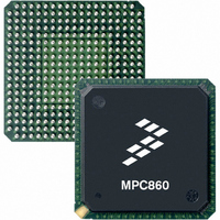
MPC859TZP100A Freescale Semiconductor, MPC859TZP100A Datasheet - Page 15

MPC859TZP100A
Manufacturer Part Number
MPC859TZP100A
Description
IC MPU POWERQUICC 100MHZ 357PBGA
Manufacturer
Freescale Semiconductor
Datasheet
1.MPC859DSLCVR50A.pdf
(96 pages)
Specifications of MPC859TZP100A
Processor Type
MPC8xx PowerQUICC 32-Bit
Speed
100MHz
Voltage
1.8V
Mounting Type
Surface Mount
Package / Case
357-PBGA
Lead Free Status / RoHS Status
Contains lead / RoHS non-compliant
Features
-
Available stocks
Company
Part Number
Manufacturer
Quantity
Price
Company:
Part Number:
MPC859TZP100A
Manufacturer:
MOT
Quantity:
12 388
Company:
Part Number:
MPC859TZP100A
Manufacturer:
MOTOLOLA
Quantity:
885
Company:
Part Number:
MPC859TZP100A
Manufacturer:
Freescale Semiconductor
Quantity:
10 000
8
This section provides design considerations for the MPC866/859 power supply. The MPC866/859 has a core voltage
(VDDL) and PLL voltage (VDDSYN) that operates at a lower voltage than the I/O voltage VDDH. The I/O section
of the MPC866/859 is supplied with 3.3 V across VDDH and V
Signals PA[0:15], PB[14:31], PC[4:15], PD[3:15], TDI, TDO, TCK, TRST_B, TMS, MII_TXEN, and MII_MDIO
are 5-V tolerant. All inputs cannot be more than 2.5 V greater than VDDH. In addition, 5-V tolerant pins cannot
exceed 5.5 V and the remaining input pins cannot exceed 3.465 V. This restriction applies to power up/down and
normal operation.
One consequence of multiple power supplies is that when power is initially applied the voltage rails ramp up at
different rates. The rates depend on the nature of the power supply, the type of load on each power supply, and the
manner in which different voltages are derived. The following restrictions apply:
These cautions are necessary for the long term reliability of the part. If they are violated, the electrostatic discharge
(ESD) protection diodes are forward-biased and excessive current can flow through these diodes. If the system
power supply design does not control the voltage sequencing, the circuit shown in
these requirements. The MUR420 Schottky diodes control the maximum potential difference between the external
bus and core power supplies on powerup and the 1N5820 diodes regulate the maximum potential difference on
powerdown.
9
Each V
Furthermore, each GND pin should be provided with a low-impedance path to ground. The power supply pins drive
distinct groups of logic on chip. The V
bypass capacitors located as close as possible to the four sides of the package. Each board designed should be
characterized and additional appropriate decoupling capacitors should be used if required. The capacitor leads and
associated printed-circuit traces connecting to chip V
At a minimum, a four-layer board employing two inner layers as V
All output pins on the MPC866/859 have fast rise and fall times. Printed-circuit (PC) trace interconnection length
should be minimized in order to minimize undershoot and reflections caused by these fast output switching times.
Freescale Semiconductor
•
•
Power Supply and Power Sequencing
Layout Practices
DD
VDDL must not exceed VDDH during power up and power down.
VDDL must not exceed 1.9 V and VDDH must not exceed 3.465 V.
pin on the MPC866/859 should be provided with a low-impedance path to the board’s supply.
Figure 4. Example Voltage Sequencing Circuit
MPC866/MPC859 Hardware Specifications, Rev. 2
DD
VDDH
power supply should be bypassed to ground using at least four 0.1 µF
DD
MUR420
and GND should be kept to less than 1/2” per capacitor lead.
1N5820
SS
(GND).
DD
VDDL
and GND planes should be used.
Power Supply and Power Sequencing
Figure 4
can be added to meet
15


