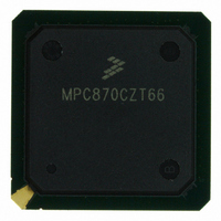
MPC870CZT66 Freescale Semiconductor, MPC870CZT66 Datasheet - Page 12

MPC870CZT66
Manufacturer Part Number
MPC870CZT66
Description
IC MPU POWERQUICC 66MHZ 256PBGA
Manufacturer
Freescale Semiconductor
Datasheet
1.MPC870VR80.pdf
(84 pages)
Specifications of MPC870CZT66
Processor Type
MPC8xx PowerQUICC 32-Bit
Speed
66MHz
Voltage
3.3V
Mounting Type
Surface Mount
Package / Case
256-PBGA
Family Name
MPC8xx
Device Core
PowerQUICC
Device Core Size
32b
Frequency (max)
66MHz
Instruction Set Architecture
RISC
Supply Voltage 1 (typ)
1.8V
Operating Supply Voltage (max)
1.9V
Operating Supply Voltage (min)
1.7V
Operating Temp Range
-40C to 100C
Operating Temperature Classification
Industrial
Mounting
Surface Mount
Pin Count
256
Package Type
BGA
Lead Free Status / RoHS Status
Contains lead / RoHS non-compliant
Features
-
Lead Free Status / Rohs Status
Not Compliant
Available stocks
Company
Part Number
Manufacturer
Quantity
Price
Company:
Part Number:
MPC870CZT66
Manufacturer:
MOT
Quantity:
12 388
Company:
Part Number:
MPC870CZT66
Manufacturer:
Freescale Semiconductor
Quantity:
10 000
Thermal Calculation and Measurement
1
2
3
4
5
6
7
For the following discussions, P
drivers.
7.1
An estimation of the chip junction temperature, T
where:
The junction-to-ambient thermal resistance is an industry standard value that provides a quick and easy
estimation of thermal performance. However, the answer is only an estimate; test cases have demonstrated
that errors of a factor of two (in the quantity T
12
Output high voltage, I
open-drain pins)
Output low voltage
I
I
I
I
I
OL
OL
OL
OL
OL
The difference between V
The signals PA[0:15], PB[14:31], PC[4:15], PD[3:15], PE(14:31), TDI, TDO, TCK, TRST, TMS, MII1_TXEN, and MII_MDIO are
5-V tolerant. The minimum voltage is still 2.0 V.
V
Input capacitance is periodically sampled.
A(0:31), TSIZ0/REG, TSIZ1, D(0:31), IRQ(2:4), IRQ6, RD/WR, BURST, IP_B(0:1), PA(0:4), PA(6:7), PA(10:11), PA15, PB19,
PB(23:31), PC(6:7), PC(10:13), PC15, PD8, PE(14:31), MII1_CRS, MII_MDIO, MII1_TXEN, and MII1_COL.
BDIP/GPL_B(5), BR, BG, FRZ/IRQ6, CS(0:7), WE(0:3), BS_A(0:3), GPL_A0/GPL_B0, OE/GPL_A1/GPL_B1,
GPL_A(2:3)/GPL_B(2:3)/CS(2:3), UPWAITA/GPL_A4, UPWAITB/GPL_B4, GPL_A5, ALE_A, CE1_A, CE2_A, OP(0:3), and
BADDR(28:30).
IL
= 2.0 mA (CLKOUT)
= 3.2 mA
= 5.3 mA
= 7.0 mA (TXD1/PA14, TXD2/PA12)
= 8.9 mA (TS, TA, TEA, BI, BB, HRESET, SRESET)
(max) for the I
Thermal Calculation and Measurement
T
R
P
A
D
θJA
Estimation with Junction-to-Ambient Thermal Resistance
= ambient temperature (°C)
= power dissipation in package
5
6
= package junction-to-ambient thermal resistance (°C/W)
T
J
2
C interface is 0.8 V rather than the 1.5 V as specified in the I
= T
OH
A
= –2.0 mA, V
+ (R
Characteristic
DDL
MPC875/MPC870 PowerQUICC™ Hardware Specifications, Rev. 4
and V
θJA
Table 6. DC Electrical Specifications (continued)
The V
× P
DDSYN
DDH
D
= (V
D
= 3.0 V (except XTAL and
)
DDSYN
cannot be more than 100 mV.
DDL
× I
power dissipation is negligible.
J
DDL
– T
NOTE
J
, in °C can be obtained from the following equation:
) + P
A
) are possible.
I/O
, where P
Symbol
V
V
OH
OL
2
I/O
C standard.
is the power dissipation of the I/O
Min
2.4
—
Freescale Semiconductor
Max
0.5
—
Unit
V
V


