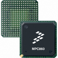
MPC860TCZQ50D4 Freescale Semiconductor, MPC860TCZQ50D4 Datasheet - Page 41

MPC860TCZQ50D4
Manufacturer Part Number
MPC860TCZQ50D4
Description
IC MPU POWERQUICC 50MHZ 357PBGA
Manufacturer
Freescale Semiconductor
Series
PowerQUICC Ir
Datasheet
1.MC860DECVR50D4R2.pdf
(80 pages)
Specifications of MPC860TCZQ50D4
Processor Type
MPC8xx PowerQUICC 32-Bit
Speed
50MHz
Voltage
3.3V
Mounting Type
Surface Mount
Package / Case
357-PBGA
Processor Series
MPC8xx
Core
MPC8xx
Data Bus Width
32 bit
Maximum Clock Frequency
50 MHz
Operating Supply Voltage
2.5 V, 3.3 V
Maximum Operating Temperature
+ 95 C
Mounting Style
SMD/SMT
Minimum Operating Temperature
- 40 C
Core Size
32 Bit
Program Memory Size
8KB
Cpu Speed
50MHz
Embedded Interface Type
Ethernet, I2C, SPI, UART
Digital Ic Case Style
BGA
No. Of Pins
357
Rohs Compliant
No
Family Name
MPC8xx
Device Core
PowerQUICC
Device Core Size
32b
Frequency (max)
50MHz
Instruction Set Architecture
RISC
Supply Voltage 1 (typ)
2.5/3.3V
Operating Supply Voltage (max)
3.465/3.6V
Operating Supply Voltage (min)
2/3.135V
Operating Temp Range
-40C to 95C
Operating Temperature Classification
Industrial
Mounting
Surface Mount
Pin Count
357
Package Type
BGA
Lead Free Status / RoHS Status
Contains lead / RoHS non-compliant
Features
-
Lead Free Status / Rohs Status
Lead free / RoHS Compliant
Available stocks
Company
Part Number
Manufacturer
Quantity
Price
Company:
Part Number:
MPC860TCZQ50D4
Manufacturer:
Freescale Semiconductor
Quantity:
10 000
Figure 34
10 IEEE 1149.1 Electrical Specifications
Table 13
Freescale Semiconductor
Num
J82
J83
J84
J85
J86
J87
J88
J89
J90
J91
J92
J93
J94
J95
J96
TCK cycle time
TCK clock pulse width measured at 1.5 V
TCK rise and fall times
TMS, TDI data setup time
TMS, TDI data hold time
TCK low to TDO data valid
TCK low to TDO data invalid
TCK low to TDO high impedance
TRST assert time
TRST setup time to TCK low
TCK falling edge to output valid
TCK falling edge to output valid out of high impedance
TCK falling edge to output high impedance
Boundary scan input valid to TCK rising edge
TCK rising edge to boundary scan input invalid
DSCK, DSDI
provides the JTAG timings for the MPC860 shown in
provides the reset timing for the debug port configuration.
CLKOUT
SRESET
MPC860 PowerQUICC™ Family Hardware Specifications, Rev. 8
Figure 34. Reset Timing—Debug Port Configuration
Characteristic
R80
Table 13. JTAG Timing
R70
R81
Figure 35
R82
R80
through
IEEE 1149.1 Electrical Specifications
100.00
100.00
40.00
25.00
40.00
50.00
50.00
0.00
5.00
0.00
Min
All Frequencies
—
—
—
—
—
R81
Figure
38.
10.00
27.00
20.00
50.00
50.00
50.00
Max
—
—
—
—
—
—
—
—
—
Unit
ns
ns
ns
ns
ns
ns
ns
ns
ns
ns
ns
ns
ns
ns
ns
41


