MPC8343VRAGDB Freescale Semiconductor, MPC8343VRAGDB Datasheet - Page 23
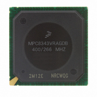
MPC8343VRAGDB
Manufacturer Part Number
MPC8343VRAGDB
Description
IC MPU POWERQUICC II 620-PBGA
Manufacturer
Freescale Semiconductor
Series
PowerQUICC II PROr
Datasheet
1.MPC8343VRAGDB.pdf
(79 pages)
Specifications of MPC8343VRAGDB
Processor Type
MPC83xx PowerQUICC II Pro 32-Bit
Speed
400MHz
Voltage
1.2V
Mounting Type
Surface Mount
Package / Case
620-PBGA
Processor Series
MPC8xxx
Core
e300
Data Bus Width
32 bit
Development Tools By Supplier
MPC8349E-MITXE
Maximum Clock Frequency
400 MHz
Maximum Operating Temperature
+ 105 C
Mounting Style
SMD/SMT
I/o Voltage
1.8 V, 2.5 V, 3.3 V
Minimum Operating Temperature
0 C
Core Size
32 Bit
Program Memory Size
64KB
Cpu Speed
400MHz
Embedded Interface Type
I2C, SPI, USB, UART
Digital Ic Case Style
BGA
No. Of Pins
620
Rohs Compliant
Yes
Family Name
MPC83xx
Device Core
PowerQUICC II Pro
Device Core Size
32b
Frequency (max)
400MHz
Instruction Set Architecture
RISC
Supply Voltage 1 (typ)
1.2V
Operating Supply Voltage (max)
1.26V
Operating Supply Voltage (min)
1.14V
Operating Temp Range
0C to 105C
Operating Temperature Classification
Commercial
Mounting
Surface Mount
Pin Count
620
Package Type
BGA
For Use With
CWH-PPC-8343N-VX - KIT EVAL SYSTEM QUICCSTART 8248CWH-PPC-8343N-VE - EVALUATION SYSTEM QUICC MPC8343E
Lead Free Status / RoHS Status
Lead free / RoHS Compliant
Features
-
Lead Free Status / Rohs Status
Lead free / RoHS Compliant
Available stocks
Company
Part Number
Manufacturer
Quantity
Price
Company:

Part Number:
MPC8343VRAGDB
Manufacturer:
Freescale Semiconductor
Quantity:
135
Company:
Part Number:
MPC8343VRAGDB
Manufacturer:
Freescale Semiconductor
Quantity:
10 000
Part Number:
MPC8343VRAGDB
Manufacturer:
FREESCALE
Quantity:
20 000


8.2
The AC timing specifications for MII, RGMII, and RTBI are presented in this section.
8.2.1
This section describes the MII transmit and receive AC timing specifications.
8.2.1.1
Table 25
Figure 8
Freescale Semiconductor
At recommended operating conditions with LV
TX_CLK clock period 10 Mbps
TX_CLK clock period 100 Mbps
TX_CLK duty cycle
TX_CLK to MII data TXD[3:0], TX_ER, TX_EN delay
TX_CLK data clock rise (20%–80%)
TX_CLK data clock fall (80%–20%)
Note:
1. The symbols for timing specifications follow the pattern of t
and t
(MT) for the time t
symbol is based on two to three letters representing the clock of a particular function. For example, the subscript of t
represents the MII(M) transmit (TX) clock. For rise and fall times, the latter convention is used with the appropriate letter:
R (rise) or F (fall).
(first two letters of functional block)(reference)(state)(signal)(state)
shows the MII transmit AC timing diagram.
provides the MII transmit AC timing specifications.
MII, RGMII, and RTBI AC Timing Specifications
MPC8343EA PowerQUICC II Pro Integrated Host Processor Hardware Specifications, Rev. 10
MII AC Timing Specifications
MII Transmit AC Timing Specifications
TXD[3:0]
Parameter/Condition
TX_CLK
MTX
TX_EN
TX_ER
clock reference (K) going high (H) until data outputs (D) are invalid (X). In general, the clock reference
Table 25. MII Transmit AC Timing Specifications
Figure 8. MII Transmit AC Timing Diagram
t
MTXH
DD
/OV
t
DD
MTX
of 3.3 V ± 10%.
for outputs. For example, t
(first two letters of functional block)(signal)(state)(reference)(state)
t
t
MTKHDX
t
Symbol
MTXH/
MTXF
t
MTKHDX
t
t
t
t
MTXR
MTXF
MTX
MTX
t
MTX
1
t
MTXR
Ethernet: Three-Speed Ethernet, MII Management
Min
1.0
1.0
35
—
—
1
MTKHDX
Typ
400
symbolizes MII transmit timing
40
—
—
—
5
Max
4.0
4.0
65
15
—
—
for inputs
MTX
Unit
ns
ns
ns
ns
ns
%
23
Related parts for MPC8343VRAGDB
Image
Part Number
Description
Manufacturer
Datasheet
Request
R

Part Number:
Description:
Manufacturer:
Freescale Semiconductor, Inc
Datasheet:
Part Number:
Description:
Manufacturer:
Freescale Semiconductor, Inc
Datasheet:
Part Number:
Description:
Manufacturer:
Freescale Semiconductor, Inc
Datasheet:
Part Number:
Description:
Manufacturer:
Freescale Semiconductor, Inc
Datasheet:
Part Number:
Description:
Manufacturer:
Freescale Semiconductor, Inc
Datasheet:
Part Number:
Description:
Manufacturer:
Freescale Semiconductor, Inc
Datasheet:
Part Number:
Description:
Manufacturer:
Freescale Semiconductor, Inc
Datasheet:
Part Number:
Description:
Manufacturer:
Freescale Semiconductor, Inc
Datasheet:
Part Number:
Description:
Manufacturer:
Freescale Semiconductor, Inc
Datasheet:
Part Number:
Description:
Manufacturer:
Freescale Semiconductor, Inc
Datasheet:
Part Number:
Description:
Manufacturer:
Freescale Semiconductor, Inc
Datasheet:
Part Number:
Description:
Manufacturer:
Freescale Semiconductor, Inc
Datasheet:
Part Number:
Description:
Manufacturer:
Freescale Semiconductor, Inc
Datasheet:
Part Number:
Description:
Manufacturer:
Freescale Semiconductor, Inc
Datasheet:
Part Number:
Description:
Manufacturer:
Freescale Semiconductor, Inc
Datasheet: