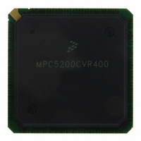
MPC5200CVR400 Freescale Semiconductor, MPC5200CVR400 Datasheet - Page 14

MPC5200CVR400
Manufacturer Part Number
MPC5200CVR400
Description
IC MPU 32BIT 400MHZ PPC 272-PBGA
Manufacturer
Freescale Semiconductor
Datasheet
1.MPC5200CVR400B.pdf
(80 pages)
Specifications of MPC5200CVR400
Processor Type
MPC52xx PowerPC 32-Bit
Speed
400MHz
Voltage
1.5V
Mounting Type
Surface Mount
Package / Case
272-PBGA
Family Name
MPC52xx
Device Core
PowerPC
Device Core Size
32b
Frequency (max)
400MHz
Instruction Set Architecture
RISC
Operating Supply Voltage (max)
1.58V
Operating Supply Voltage (min)
1.42V
Operating Temp Range
-40C to 85C
Operating Temperature Classification
Industrial
Mounting
Surface Mount
Pin Count
272
Package Type
BGA
Lead Free Status / RoHS Status
Lead free / RoHS Compliant
Features
-
Lead Free Status / Rohs Status
Compliant
Available stocks
Company
Part Number
Manufacturer
Quantity
Price
Company:
Part Number:
MPC5200CVR400
Manufacturer:
FREESCAL
Quantity:
200
Company:
Part Number:
MPC5200CVR400
Manufacturer:
Freescale Semiconductor
Quantity:
10 000
Company:
Part Number:
MPC5200CVR400B
Manufacturer:
Marvell
Quantity:
1 001
Company:
Part Number:
MPC5200CVR400B
Manufacturer:
FREESCAL
Quantity:
200
Company:
Part Number:
MPC5200CVR400B
Manufacturer:
Freescale Semiconductor
Quantity:
10 000
Part Number:
MPC5200CVR400B
Manufacturer:
FREESCALE
Quantity:
20 000
Company:
Part Number:
MPC5200CVR400BM62C
Manufacturer:
FRRESCAL..
Quantity:
2 831
Electrical and Thermal Characteristics
3.2.4
The internal clocking of the G2_LE core is generated from and synchronized to the system clock by means
of a voltage-controlled core PLL.
3.3
Hyperlinks to the indicated timing specification sections are provided below.
AC Test Timing Conditions:
Unless otherwise noted, all test conditions are as follows:
14
NOTES:
1
2
3
G2_LE frequency
G2_LE cycle time
G2_LE VCO frequency
G2_LE input clock frequency
G2_LE input clock cycle time
G2_LE input clock jitter
G2_LE PLL relock time
The XLB_CLK frequency and G2_LE PLL Configuration bits must be chosen such that the resulting system
frequencies, CPU (core) frequency, and G2_LE PLL (VCO) frequency do not exceed their respective maximum or
minimum operating frequencies.
This represents total input jitter - short term and long term combined - and is guaranteed by design. Two different
types of jitter can exist on the input to core_sysclk, systemic and true random jitter. True random jitter is rejected, but
the PLL. Systemic jitter will be passed into and through the PLL to the internal clock circuitry, directly reducing the
operating frequency.
Relock time is guaranteed by design and characterization. PLL-relock time is the maximum amount of time required
for the PLL lock after a stable Vdd and core_sysclk are reached during the power-on reset sequence. This
specification also applies when the PLL has been disabled and subsequently re-enabled during sleep modes.
•
•
•
•
•
•
•
•
•
AC Electrical Characteristics
G2_LE Core PLL Electrical Characteristics
AC Operating Frequency Data
Clock AC Specifications
Resets
External Interrupts
SDRAM
PCI
Local Plus Bus
ATA
Ethernet
Characteristic
Table 11. G2_LE PLL Specifications
f
t
Symbol
f
XLB_CLK
XLB_CLK
VCOcore
f
t
t
t
core
core
jitter
lock
MPC5200 Data Sheet, Rev. 4
Notes
(1)
(1)
1
2
3
•
•
•
•
•
•
•
•
2.85
2.73
Min
400
50
25
—
—
USB
SPI
MSCAN
I
J1850
PSC
GPIOs and Timers
IEEE 1149.1 (JTAG) AC Specifications
2
C
Typical
—
—
—
—
—
—
—
1200
Max
40.0
50.0
550
367
150
100
Freescale Semiconductor
MHz
MHz
MHz
Unit
ns
ns
ps
µs
SpecID
O4.1
O4.2
O4.3
O4.4
O4.5
O4.6
O4.7


