Z8018233FSG Zilog, Z8018233FSG Datasheet - Page 95
Z8018233FSG
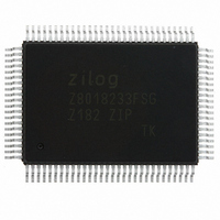
Manufacturer Part Number
Z8018233FSG
Description
IC 33MHZ STATIC MIMIC 100-QFP
Manufacturer
Zilog
Datasheet
1.Z8018233FSG.pdf
(109 pages)
Specifications of Z8018233FSG
Processor Type
Z180
Features
Smart Peripheral Controller
Speed
33MHz
Voltage
5V
Mounting Type
Surface Mount
Package / Case
100-QFP
Processor Series
Z8018xx
Core
Z80
Data Bus Width
8 bit
Program Memory Type
ROMLess
Interface Type
UART
Maximum Clock Frequency
33 MHz
Number Of Programmable I/os
24
Number Of Timers
2
Operating Supply Voltage
4.5 V to 5.5 V
Maximum Operating Temperature
+ 70 C
Mounting Style
SMD/SMT
Minimum Operating Temperature
0 C
Lead Free Status / RoHS Status
Lead free / RoHS Compliant
Other names
269-4694
Z8018233FSG
Z8018233FSG
Available stocks
Company
Part Number
Manufacturer
Quantity
Price
Company:

Part Number:
Z8018233FSG
Manufacturer:
Zilog
Quantity:
100


Notes:
These AC parameter values are preliminary and subject to change without notice.
[1] RxC is /RTxC or /TRxC, whichever is supplying the receive clock.
[2] TxC is /TRxC or /RTxC, whichever is supplying the transmit clock.
[3] Both /RTxC and /SYNC have 30 pF capacitors to ground connected to them.
[4] Synchronization of RxC to PCLK is eliminated in divide by four operation.
[5] Parameter applies only to FM encoding/decoding.
[6] Parameter applies only for transmitter and receiver; DPLL and baud
[7] The maximum receive or transmit data rate is 1/4 PCLK.
[8] Applies to DPLL clock source only. Maximum data rate of 1/4 PCLK
DS971820600
Zilog
No.
1
2
3
4
5
6
7
8
9
10
11
12
13
14
15
16a
16b
17
18
19
20
21
22
still applies. DPLL clock should have a 50% duty cycle.
rate generator timing requirements are identical to case PCLK requirements.
Symbol
TdPC(REQ)
TdPC(W)
TsRxC(PC)
TsRxD(RxCr)
ThRxD(RxCr)
TsRxD(RxCf)
ThRxD(RxCf)
TsSY(RxC)
ThSY(RXC)
TsTxC(PC)
TdTxCf(TXD)
TdTxCr(TXD)
TdTxD(TRX)
TwRTxh
TwRTxI
TcRTx
TxRx(DPLL)
TcRTxx
TwTRxh
TwTRxl
TcTRx
TwExT
TwSY
Table C. Z85230 General Timing Table
Parameter
/PCLK to W/REQ Valid
/PCLK to Wait Inactive
/RxC to /PCLK Setup Time
RxD to /RxC Setup Time
RxD to /RxC Hold Time
RxD to /RxC Setup Time
RxD to /RxC Hold Time
/SYNC to /RxC Setup Time
/SYNC to/RxC Hold Time
/TxC to /PCLK Setup Time
/TxC to TxD Delay
/TxC to TxD Delay
TxD to TRxC Delay
RTxC High Width
TRxC Low Width
RTxC Cycle Time
DPLL Cycle Time Min
Crystal Osc. Period
TRxC High Width
TRxC Low Width
TRxC Cycle Time
DCD or CTS Pulse Width
SYNC Pulse Width
PS009801-0301
P R E L I M I N A R Y
5TcPc
Min
N/A
–90
N/A
200
200
50
45
45
70
70
61
70
70
60
60
0
20 MHz
1000
Max
170
70
70
70
70
0
Z
ILOG
I
NTELLIGENT
Z80182/Z8L182
Notes
[1,4]
[1,5]
[1,5]
[2,4]
[2,5]
[6,7]
[7,8]
[6,7]
[1]
[1]
[1]
[1]
[2]
[6]
[6]
[3]
[6]
[6]
P
ERIPHERAL
3-95
Related parts for Z8018233FSG
Image
Part Number
Description
Manufacturer
Datasheet
Request
R

Part Number:
Description:
Z80182 ZIP APPLICATION BOARD
Manufacturer:
Zilog
Datasheet:

Part Number:
Description:
Communication Controllers, ZILOG INTELLIGENT PERIPHERAL CONTROLLER (ZIP)
Manufacturer:
Zilog, Inc.
Datasheet:

Part Number:
Description:
KIT DEV FOR Z8 ENCORE 16K TO 64K
Manufacturer:
Zilog
Datasheet:

Part Number:
Description:
KIT DEV Z8 ENCORE XP 28-PIN
Manufacturer:
Zilog
Datasheet:

Part Number:
Description:
DEV KIT FOR Z8 ENCORE 8K/4K
Manufacturer:
Zilog
Datasheet:

Part Number:
Description:
KIT DEV Z8 ENCORE XP 28-PIN
Manufacturer:
Zilog
Datasheet:
Part Number:
Description:
DEV KIT FOR Z8 ENCORE 4K TO 8K
Manufacturer:
Zilog
Datasheet:
Part Number:
Description:
CMOS Z8 microcontroller. ROM 16 Kbytes, RAM 256 bytes, speed 16 MHz, 32 lines I/O, 3.0V to 5.5V
Manufacturer:
Zilog, Inc.
Datasheet:
Part Number:
Description:
Low-cost microcontroller. 512 bytes ROM, 61 bytes RAM, 8 MHz
Manufacturer:
Zilog, Inc.
Datasheet:
Part Number:
Description:
Z8 4K OTP Microcontroller
Manufacturer:
Zilog, Inc.
Datasheet:
Part Number:
Description:
CMOS SUPER8 ROMLESS MCU
Manufacturer:
Zilog, Inc.
Datasheet:
Part Number:
Description:
SL1866 CMOSZ8 OTP Microcontroller
Manufacturer:
Zilog, Inc.
Datasheet:
Part Number:
Description:
SL1866 CMOSZ8 OTP Microcontroller
Manufacturer:
Zilog, Inc.
Datasheet:
Part Number:
Description:
OTP (KB) = 1, RAM = 125, Speed = 12, I/O = 14, 8-bit Timers = 2, Comm Interfaces Other Features = Por, LV Protect, Voltage = 4.5-5.5V
Manufacturer:
Zilog, Inc.
Datasheet: