CY7C63743-PXC Cypress Semiconductor Corp, CY7C63743-PXC Datasheet - Page 8

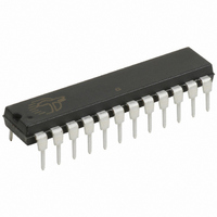
CY7C63743-PXC
Manufacturer Part Number
CY7C63743-PXC
Description
IC MCU 8K USB/PS2 LS 24DIP
Manufacturer
Cypress Semiconductor Corp
Series
enCoRe™r
Specifications of CY7C63743-PXC
Applications
USB Microcontroller
Core Processor
M8B
Program Memory Type
OTP (8 kB)
Controller Series
CY7C637xx
Ram Size
256 x 8
Interface
PS2, USB
Number Of I /o
16
Voltage - Supply
4 V ~ 5.5 V
Operating Temperature
0°C ~ 70°C
Mounting Type
Through Hole
Package / Case
24-DIP (0.300", 7.62mm)
Lead Free Status / RoHS Status
Lead free / RoHS Compliant
Other names
428-1621
Available stocks
Company
Part Number
Manufacturer
Quantity
Price
Company:
Part Number:
CY7C63743-PXC
Manufacturer:
TI
Quantity:
12 749
Data Memory Organization
The CY7C637xxC microcontrollers provide 256 bytes of data RAM. In normal usage, the SRAM is partitioned into four areas: program
stack, data stack, user variables and USB endpoint FIFOs as shown below.
I/O Register Summary
I/O registers are accessed via the I/O Read (IORD) and I/O Write
(IOWR, IOWX) instructions. IORD reads the selected port into
the accumulator. IOWR writes data from the accumulator to the
selected port. Indexed I/O Write (IOWX) adds the contents of X
to the address in the instruction to form the port address and
writes data from the accumulator to the specified port. Note that
Table 1. I/O Register Summary
Document #: 38-08022 Rev. *D
Port 0 Data
Port 1 Data
Port 2 Data
Port 0 Interrupt Enable
Port 1 Interrupt Enable
Port 0 Interrupt Polarity
Port 1 Interrupt Polarity
Port 0 Mode0
Port 0 Mode1
Port 1 Mode0
Port 1 Mode1
8-bit DSP
8-bit DSP
Register Name
(User’s firmware moves DSP)
After reset
8-bit PSP
Top of RAM Memory
I/O Address
0x0A
0x0C
0x0D
0x00
0x01
0x02
0x04
0x05
0x06
0x07
0x0B
User Selected
Figure 2. Data Memory Organization
Address
0xE8
0xFF
0x00
0xF0
0xF8
Read/Write
R/W
R/W
W
W
W
W
W
W
W
W
R
User Variables
USB FIFO for Address A endpoint 2
USB FIFO for Address A endpoint 1
USB FIFO for Address A endpoint 0
GPIO Port 0
GPIO Port 1
Auxiliary input register for D+, D–, VREG, XTALIN
Interrupt enable for pins in Port 0
Interrupt enable for pins in Port 1
Interrupt polarity for pins in Port 0
Interrupt polarity for pins in Port 1
Controls output configuration for Port 0
Controls output configuration for Port 1
specifying address 0 with IOWX (e.g., IOWX 0h) means the I/O
port is selected solely by the contents of X.
Note: All bits of all registers are cleared to all zeros on reset,
except the Processor Status and Control Register
registers not listed are reserved, and should never be written by
firmware. All bits marked as reserved should always be written
as 0 and be treated as undefined by reads.
Program Stack Growth
Data Stack Growth
Function
CY7C63722C
CY7C63723C
CY7C63743C
(Figure
Page 8 of 53
Fig
37
38
39
11
12
7
8
9
33). All
[+] Feedback


