AT43USB320A-AC Atmel, AT43USB320A-AC Datasheet - Page 8
AT43USB320A-AC
Manufacturer Part Number
AT43USB320A-AC
Description
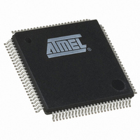
IC USB MCU EMBED HUB AVR 100LQFP
Manufacturer
Atmel
Series
AVR®r
Datasheet
1.AT43USB320A-AC.pdf
(115 pages)
Specifications of AT43USB320A-AC
Applications
USB Hub/Microcontroller
Core Processor
AVR
Controller Series
AT43USB
Ram Size
512 x 8
Interface
SPI Serial, USB, UART
Number Of I /o
32
Voltage - Supply
4.4 V ~ 5.25 V
Operating Temperature
0°C ~ 70°C
Mounting Type
Surface Mount
Package / Case
100-LQFP
Lead Free Status / RoHS Status
Contains lead / RoHS non-compliant
Program Memory Type
-
Available stocks
Company
Part Number
Manufacturer
Quantity
Price


The General-
purpose
Register File
8
AT43USB320A
During interrupts and subroutine calls, the return address Program Counter (PC) is stored on
the stack. The stack is effectively allocated in the general data SRAM, and consequently, the
stack size is only limited by the total SRAM size and the usage of the SRAM. All user pro-
grams must initialize the Stack Pointer (SP) in the reset routine (before subroutines or
interrupts are executed). The 10-bit SP is read/write accessible in the I/O space.
The 512-byte data SRAM can be easily accessed through the five different addressing modes
supported in the AVR architecture.
The memory spaces in the AVR architecture are all linear and regular memory maps. A flexi-
ble interrupt module has its control registers in the I/O space with an additional global interrupt
enable bit in the status register. All interrupts have a separate interrupt vector in the interrupt
vector table at the beginning of the program memory. The interrupts have priority in accor-
dance with their interrupt vector position. The lower the interrupt vector address, the higher the
priority.
Table 1. AVR CPU General Purpose Working Register
All register operating instructions in the instruction set have direct and single cycle access to
all registers. The only exception is the five constant arithmetic and logic instructions SBCI,
SUBI, CPI, ANDI, and ORI between a constant and a register, and the LDI instruction for load
immediate constant data. These instructions apply to the second half of the registers in the
register file – R16..R31. The general SBC, SUB, CP, AND, and OR and all other operations
between two registers or on a single register apply to the entire register file.
As shown in Table 1, each register is also assigned a data memory address, mapping them
directly into the first 32 locations of the user Data Space. Although not being physically imple-
mented as SRAM locations, this memory organization provides great flexibility in access of the
registers, as the X-, Y-, and Z-registers can be set to index any register in the file.
Register
R0
R1
R2
..
R13
R14
R15
R16
R17
..
R26
R27
R28
R29
R30
R31
Address
$00
$01
$02
$0D
$0E
$0F
$10
$11
$1A
$1B
$1C
$1D
$1E
$1F
Comment
X-register low byte
X-register high byte
Y-register low byte
Y-register high byte
Z-register low byte
Z-register high byte
1443E–USB–4/04
Related parts for AT43USB320A-AC
Image
Part Number
Description
Manufacturer
Datasheet
Request
R

Part Number:
Description:
DEV KIT FOR AVR/AVR32
Manufacturer:
Atmel
Datasheet:

Part Number:
Description:
INTERVAL AND WIPE/WASH WIPER CONTROL IC WITH DELAY
Manufacturer:
ATMEL Corporation
Datasheet:
Part Number:
Description:
Low-Voltage Voice-Switched IC for Hands-Free Operation
Manufacturer:
ATMEL Corporation
Datasheet:
Part Number:
Description:
MONOLITHIC INTEGRATED FEATUREPHONE CIRCUIT
Manufacturer:
ATMEL Corporation
Datasheet:
Part Number:
Description:
AM-FM Receiver IC U4255BM-M
Manufacturer:
ATMEL Corporation
Datasheet:
Part Number:
Description:
Monolithic Integrated Feature Phone Circuit
Manufacturer:
ATMEL Corporation
Datasheet:
Part Number:
Description:
Multistandard Video-IF and Quasi Parallel Sound Processing
Manufacturer:
ATMEL Corporation
Datasheet:
Part Number:
Description:
High-performance EE PLD
Manufacturer:
ATMEL Corporation
Datasheet:
Part Number:
Description:
8-bit Flash Microcontroller
Manufacturer:
ATMEL Corporation
Datasheet:
Part Number:
Description:
2-Wire Serial EEPROM
Manufacturer:
ATMEL Corporation
Datasheet: