MM908E626AVDWB Freescale Semiconductor, MM908E626AVDWB Datasheet - Page 21
MM908E626AVDWB
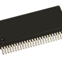
Manufacturer Part Number
MM908E626AVDWB
Description
IC STEPPER MOTOR DRIVER 54-SOIC
Manufacturer
Freescale Semiconductor
Type
Stepper Motor Driverr
Datasheet
1.MM908E626AVEK.pdf
(44 pages)
Specifications of MM908E626AVDWB
Applications
Automotive Mirror Control
Core Processor
HC08
Program Memory Type
FLASH (16 kB)
Controller Series
908E
Ram Size
512 x 8
Interface
SCI, SPI
Number Of I /o
13
Voltage - Supply
8 V ~ 18 V
Operating Temperature
-40°C ~ 115°C
Mounting Type
Surface Mount
Package / Case
54-SOIC (7.5mm Width) Exposed Pad, 54-eSOIC, 54-HSOIC
Product
Stepper Motor Controllers / Drivers
Operating Supply Voltage
8 V to 18 V
Supply Current
20 mA
Mounting Style
SMD/SMT
Lead Free Status / Rohs Status
Lead free / RoHS Compliant
Available stocks
Company
Part Number
Manufacturer
Quantity
Price

Part Number:
MM908E626AVDWB
Manufacturer:
FREESCALE
Quantity:
20 000


RESET EXTERNAL SOURCE
External Reset Pin
SMARTMOS device by pulling down the
Reset Mask Register (RMR)
communication link between the microcontroller and the
908E626.
prepared. The falling edge on the
of a new data transfer and puts MISO in the low-impedance
mode. The first valid data are moved to MISO with the rising
edge of SPSCK.
Analog Integrated Circuit Device Data
Freescale Semiconductor
Reset
Read
Write
SPSCK
The microcontroller has the capability of resetting the
The serial peripheral interface (SPI) creates the
The interface consists of four pins (see
•
MOSI
MISO
During the inactive phase of
SS
SS
TTEST
— Slave Select
Rising edge of SPSCK
Bit 7
Change MISO/MOSI
0
Register Name and Address: RMR - $06
6
0
0
Output
5
0
0
R/W
S7
Falling edge of SPSCK
Sample MISO/MOSI
Input
4
0
0
A4
S6
SS
SS
, the new data transfer is
Read/Write, Address, Parity
A3
S5
System Status Register
3
0
0
line indicates the start
A2
S4
RST
Figure
SERIAL PERIPHERAL INTERFACE
2
0
0
A1
S3
pin.
HVRE
11):
1
0
A0
S2
Figure 11. SPI Protocol
Slave latch
register address
HTRE
S1
Bit 0
P
0
S0
X
TTEST — High Temperature Reset Test
the overtemperature shutdown limit for final test. Reset clears
the HTRE bit.
HVRE — High Voltage Reset Enable Bit
conditions. Reset clears the HVRE bit.
HTRE — High Temperature Reset Enable Bit
conditions. Reset clears the HTRE bit.
The master sends address and data, slave system status,
and data of the selected address.
SPSCK. The MOSI input is sampled on a falling edge of
SPSCK. The data transfer is only valid if exactly 16 sample
clock edges are present in the active phase of
This read / write bit is for test purposes only. It decreases
• 1 = Low temperature threshold enabled.
• 0 = Low temperature threshold disabled.
This read / write bit enables resets on high voltage
• 1 = High voltage reset enabled.
• 0 = High voltage reset disabled.
This read / write bit enables resets on high temperature
• 1 = High temperature reset enabled.
• 0 = High temperature reset disabled.
• MOSI — Master-Out Slave-In
• MISO — Master-In Slave-Out
• SPSCK — Serial Clock (maximum frequency 4.0 MHz)
A complete data transfer via the SPI consists of 2 bytes.
The MISO output changes data on a rising edge of
D7
D7
D6
D6
D5
D5
Data (Register write)
Data (Register read)
FUNCTIONAL DEVICE OPERATION
D4
D4
D3
D3
D2
D2
OPERATIONAL MODES
D1
D1
D0
D0
Slave latch
SS
.
data
908E626
21
Related parts for MM908E626AVDWB
Image
Part Number
Description
Manufacturer
Datasheet
Request
R

Part Number:
Description:
Integrated Stepper Motor Driver With Embedded Mcu And Lin Serial Communication
Manufacturer:
Freescale Semiconductor, Inc
Datasheet:
Part Number:
Description:
Manufacturer:
Freescale Semiconductor, Inc
Datasheet:
Part Number:
Description:
Manufacturer:
Freescale Semiconductor, Inc
Datasheet:
Part Number:
Description:
Manufacturer:
Freescale Semiconductor, Inc
Datasheet:
Part Number:
Description:
Manufacturer:
Freescale Semiconductor, Inc
Datasheet:
Part Number:
Description:
Manufacturer:
Freescale Semiconductor, Inc
Datasheet:
Part Number:
Description:
Manufacturer:
Freescale Semiconductor, Inc
Datasheet:
Part Number:
Description:
Manufacturer:
Freescale Semiconductor, Inc
Datasheet:
Part Number:
Description:
Manufacturer:
Freescale Semiconductor, Inc
Datasheet:
Part Number:
Description:
Manufacturer:
Freescale Semiconductor, Inc
Datasheet:
Part Number:
Description:
Manufacturer:
Freescale Semiconductor, Inc
Datasheet:
Part Number:
Description:
Manufacturer:
Freescale Semiconductor, Inc
Datasheet:
Part Number:
Description:
Manufacturer:
Freescale Semiconductor, Inc
Datasheet:
Part Number:
Description:
Manufacturer:
Freescale Semiconductor, Inc
Datasheet:
Part Number:
Description:
Manufacturer:
Freescale Semiconductor, Inc
Datasheet: