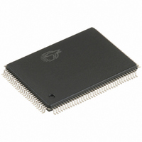
CY7C68014A-128AXC Cypress Semiconductor Corp, CY7C68014A-128AXC Datasheet - Page 38

CY7C68014A-128AXC
Manufacturer Part Number
CY7C68014A-128AXC
Description
IC MCU USB PERIPH HI SPD 128LQFP
Manufacturer
Cypress Semiconductor Corp
Series
EZ-USB FX2LP™r
Specifications of CY7C68014A-128AXC
Program Memory Type
ROMless
Package / Case
128-LQFP
Applications
USB Microcontroller
Core Processor
8051
Controller Series
CY7C680xx
Ram Size
16K x 8
Interface
I²C, USB, USART
Number Of I /o
40
Voltage - Supply
3 V ~ 3.6 V
Operating Temperature
0°C ~ 70°C
Mounting Type
Surface Mount
Processor Series
CY7C68xx
Core
8051
Data Bus Width
8 bit
Data Ram Size
16 KB
Interface Type
I2C/USART/USB
Maximum Clock Frequency
48 MHz
Number Of Programmable I/os
40
Number Of Timers
3
Maximum Operating Temperature
+ 70 C
Mounting Style
SMD/SMT
Development Tools By Supplier
CY3684
Minimum Operating Temperature
0 C
Controller Family/series
(8051) USB
Core Size
8 Bit
No. Of I/o's
40
Program Memory Size
16KB
Cpu Speed
48MHz
No. Of Timers
3
Embedded Interface Type
I2C, USART, USB
Rohs Compliant
Yes
Package
128TQFP
Device Core
8051
Family Name
FX2LP
Maximum Speed
48 MHz
Operating Supply Voltage
3.3 V
Lead Free Status / RoHS Status
Lead free / RoHS Compliant
For Use With
CY4611B - KIT USB TO ATA REFERENCE DESIGN
Lead Free Status / Rohs Status
Lead free / RoHS Compliant
Other names
428-1671
Available stocks
Company
Part Number
Manufacturer
Quantity
Price
Company:
Part Number:
CY7C68014A-128AXC
Manufacturer:
Cypress Semiconductor Corp
Quantity:
10 000
10.2 Program Memory Read
Table 15. Program Memory Read Parameters
Document #: 38-08032 Rev. *M
t
t
t
t
t
t
t
t
Notes
CL
AV
STBL
STBH
SOEL
SCSL
DSU
DH
17. CLKOUT is shown with positive polarity.
18. t
CLKOUT
Parameter
t
t
ACC1
ACC1
ACC1
A[15..0]
(24 MHz) = 3*t
(48 MHz) = 3*t
PSEN#
is computed from the above parameters as follows:
D[7..0]
CS#
OE#
[17]
1/CLKOUT Frequency
Delay from Clock to Valid Address
Clock to PSEN Low
Clock to PSEN High
Clock to OE Low
Clock to CS Low
Data Setup to Clock
Data Hold Time
CL
CL
– t
– t
t
AV
AV
AV
t
CL
– t
– t
DSU
DSU
t
SOEL
t
SCSL
= 106 ns
= 43 ns.
Description
Figure 12. Program Memory Read Timing Diagram
t
STBL
t
ACC1
[18]
data in
Min
9.6
0
0
0
0
t
STBH
t
DH
20.83
41.66
83.2
Typ
t
AV
CY7C68013A, CY7C68014A
CY7C68015A, CY7C68016A
Max
10.7
11.1
13
8
8
Unit
ns
ns
ns
ns
ns
ns
ns
ns
ns
ns
Page 38 of 62
48 MHz
24 MHz
12 MHz
Notes
[+] Feedback


