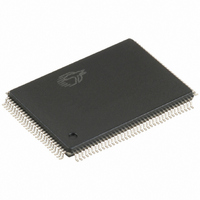
CY7C68014A-128AXC Cypress Semiconductor Corp, CY7C68014A-128AXC Datasheet - Page 15

CY7C68014A-128AXC
Manufacturer Part Number
CY7C68014A-128AXC
Description
IC MCU USB PERIPH HI SPD 128LQFP
Manufacturer
Cypress Semiconductor Corp
Series
EZ-USB FX2LP™r
Specifications of CY7C68014A-128AXC
Program Memory Type
ROMless
Package / Case
128-LQFP
Applications
USB Microcontroller
Core Processor
8051
Controller Series
CY7C680xx
Ram Size
16K x 8
Interface
I²C, USB, USART
Number Of I /o
40
Voltage - Supply
3 V ~ 3.6 V
Operating Temperature
0°C ~ 70°C
Mounting Type
Surface Mount
Processor Series
CY7C68xx
Core
8051
Data Bus Width
8 bit
Data Ram Size
16 KB
Interface Type
I2C/USART/USB
Maximum Clock Frequency
48 MHz
Number Of Programmable I/os
40
Number Of Timers
3
Maximum Operating Temperature
+ 70 C
Mounting Style
SMD/SMT
Development Tools By Supplier
CY3684
Minimum Operating Temperature
0 C
Controller Family/series
(8051) USB
Core Size
8 Bit
No. Of I/o's
40
Program Memory Size
16KB
Cpu Speed
48MHz
No. Of Timers
3
Embedded Interface Type
I2C, USART, USB
Rohs Compliant
Yes
Package
128TQFP
Device Core
8051
Family Name
FX2LP
Maximum Speed
48 MHz
Operating Supply Voltage
3.3 V
Lead Free Status / RoHS Status
Lead free / RoHS Compliant
For Use With
CY4611B - KIT USB TO ATA REFERENCE DESIGN
Lead Free Status / Rohs Status
Lead free / RoHS Compliant
Other names
428-1671
Available stocks
Company
Part Number
Manufacturer
Quantity
Price
Company:
Part Number:
CY7C68014A-128AXC
Manufacturer:
Cypress Semiconductor Corp
Quantity:
10 000
3. Pin Assignments
Figure 3-1 on page 16
types. The following pages illustrate the individual pin diagrams,
plus a combination diagram showing which of the full set of
signals are available in the 128-pin, 100-pin, and 56-pin
packages.
The signals on the left edge of the 56-pin package in
on page 16
the noted differences between the CY7C68013A/14A and the
CY7C68015A/16A.
Three modes are available in all package versions: Port, GPIF
master, and Slave FIFO. These modes define the signals on the
right edge of the diagram. The 8051 selects the interface mode
using the IFCONFIG[1:0] register bits. Port mode is the power on
default configuration.
The 100-pin package adds functionality to the 56-pin package by
adding these pins:
■
■
■
■
■
■
Document #: 38-08032 Rev. *T
PORTC or alternate GPIFADR[7:0] address signals
PORTE or alternate GPIFADR[8] address signal and seven
additional 8051 signals
Three GPIF Control signals
Four GPIF Ready signals
Nine 8051 signals (two USARTs, three timer inputs, INT4,and
INT5#)
BKPT, RD#, WR#.
are common to all versions in the FX2LP family with
identifies all signals for the five package
Figure 3-1
The 128-pin package adds the 8051 address and data buses
plus control signals. Note that two of the required signals, RD#
and WR#, are present in the 100-pin version.
In the 100-pin and 128-pin versions, an 8051 control bit can be
set to pulse the RD# and WR# pins when the 8051 reads
from/writes to PORTC. This feature is enabled by setting
PORTCSTB bit in CPUCS register.
Section 9.5
strobing function on accessing PORTC.
displays the timing diagram of the read and write
CY7C68013A, CY7C68014A
CY7C68015A, CY7C68016A
Page 15 of 67
[+] Feedback


