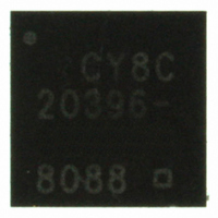
CY8C20396-24LQXI Cypress Semiconductor Corp, CY8C20396-24LQXI Datasheet - Page 28

CY8C20396-24LQXI
Manufacturer Part Number
CY8C20396-24LQXI
Description
IC CAPSENSE 19 I/O 16K 24UQFN
Manufacturer
Cypress Semiconductor Corp
Series
CapSense® Controllersr
Datasheet
1.CY8C20236-24LKXI.pdf
(39 pages)
Specifications of CY8C20396-24LQXI
Applications
Capacitive Sensing
Core Processor
M8C
Program Memory Type
FLASH (16 kB)
Controller Series
CY8C20xx6
Ram Size
2K x 8
Interface
I²C, SPI, USB
Number Of I /o
19
Voltage - Supply
1.71 V ~ 5.5 V
Operating Temperature
-40°C ~ 85°C
Mounting Type
Surface Mount
Package / Case
24-UQFN Exposed Pad, 24-HUQFN
Operating Temperature (min)
-40C
Operating Temperature (max)
85C
Technology
CMOS
Processing Unit
Microprocessor
Operating Supply Voltage (min)
1.71V
Operating Supply Voltage (typ)
1.8/2.5/3.3/5V
Operating Supply Voltage (max)
5.5V
Package Type
QFN EP
Screening Level
Industrial
Pin Count
24
Mounting
Surface Mount
Rad Hardened
No
Processor Series
CY8C20x96
Core
M8C
Data Bus Width
8 bit
Mounting Style
SMD/SMT
Development Tools By Supplier
CY3280-20X66
Lead Free Status / RoHS Status
Lead free / RoHS Compliant
For Use With
770-1000 - ISP 4PORT FOR CYPRESS PSOC MCU
Lead Free Status / Rohs Status
Details
Other names
428-2943
Available stocks
Company
Part Number
Manufacturer
Quantity
Price
Company:
Part Number:
CY8C20396-24LQXI
Manufacturer:
Maxim
Quantity:
29
AC Programming Specifications
The following table lists the guaranteed maximum and minimum specifications for the entire voltage and temperature ranges.
Table 32. AC Programming Specifications
Document Number: 001-12696 Rev. *E
T
T
T
T
F
T
T
T
T
T
T
Symbol
RSCLK
FSCLK
SSCLK
HSCLK
SCLK
ERASEB
WRITE
DSCLK
DSCLK3
DSCLK2
XRST3
SCLK (P1[1])
SDATA (P1[0])
Rise Time of SCLK
Fall Time of SCLK
Data Set up Time to Falling Edge of SCLK
Data Hold Time from Falling Edge of SCLK
Frequency of SCLK
Flash Erase Time (Block)
Flash Block Write Time
Data Out Delay from Falling Edge of SCLK 3.6 < Vdd
Data Out Delay from Falling Edge of SCLK 3.0 ≤ Vdd ≤ 3.6
Data Out Delay from Falling Edge of SCLK 1.71 ≤ Vdd ≤ 3.0
External Reset Pulse Width after Power Up Required to enter programming mode
T
RSCLK
Description
T
SSCLK
T
FSCLK
Figure 13. AC Waveform
T
HSCLK
when coming out of sleep
Conditions
T
Min
263
DSCLK
40
40
CY8C20X36/46/66/96
1
1
0
–
–
–
–
–
Typ
–
–
–
–
–
–
–
–
–
–
–
Max
130
20
20
18
25
60
85
–
–
8
–
Page 28 of 39
Units
MHz
ms
ms
ns
ns
ns
ns
ns
ns
ns
μs
[+] Feedback


