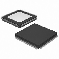
XC5210-6PQ208C Xilinx Inc, XC5210-6PQ208C Datasheet - Page 48

XC5210-6PQ208C
Manufacturer Part Number
XC5210-6PQ208C
Description
IC FPGA 324 CLB'S 208-PQFP
Manufacturer
Xilinx Inc
Series
XC5200r
Datasheet
1.XC5206-5PQ208C.pdf
(73 pages)
Specifications of XC5210-6PQ208C
Number Of Logic Elements/cells
1296
Number Of Labs/clbs
324
Number Of I /o
164
Number Of Gates
16000
Voltage - Supply
4.75 V ~ 5.25 V
Mounting Type
Surface Mount
Operating Temperature
0°C ~ 85°C
Package / Case
208-BFQFP
Lead Free Status / RoHS Status
Contains lead / RoHS non-compliant
Total Ram Bits
-
Other names
122-1149
Available stocks
Company
Part Number
Manufacturer
Quantity
Price
Company:
Part Number:
XC5210-6PQ208C
Manufacturer:
XILINX
Quantity:
88
Part Number:
XC5210-6PQ208C
Manufacturer:
XILINX/赛灵思
Quantity:
20 000
XC5200 Series Field Programmable Gate Arrays
XC5200 Guaranteed Input and Output Parameters (Pin-to-Pin)
All values listed below are tested directly, and guaranteed over the operating conditions. The same parameters can also be
derived indirectly from the Global Buffer specifications. The delay calculator uses this indirect method, and may
overestimate because of worst-case assumptions. When there is a discrepancy between these two methods, the values
listed below should be used, and the derived values should be considered conservative overestimates.
7-130
Global Clock to Output Pad (fast)
Global Clock to Output Pad (slew-limited)
Input Set-up Time (no delay) to CLB Flip-Flop
Input Hold Time (no delay) to CLB Flip-Flop
Input Set-up Time (with delay) to CLB Flip-Flop DI Input
Input Set-up Time (with delay) to CLB Flip-Flop F Input
Input Hold Time (with delay) to CLB Flip-Flop
Note:
Global Clock-to-Output Delay
1. These measurements assume that the CLB flip-flop uses a direct interconnect to or from the IOB. The INREG/ OUTREG
2. When testing outputs (fast or slew-limited), half of the outputs on one side of the device are switching.
Global Clock-to-Output Delay
& Hold
Set-up
& Hold
Set-up
Input
Set-up
& Hold
Input
Time
& Hold
Time
properties, or XACT-Performance, can be used to assure that direct connects are used. t
DI that bypasses the look-up table, which only offers direct connects to IOBs on the left and right edges of the die. t
applies to the CLB inputs F that feed the look-up table, which offers direct connect to IOBs on all four edges, as do the CLB
Q outputs.
Set-up
& Hold
Input
Time
Set-up
Input
Time
Input
Time
BUFG
IOB
BUFG
IOB
(NODELAY) Direct
(NODELAY)
BUFG
BUFG
BUFG
IOB
IOB
BUFG
BUFG
Description
Product Obsolete or Under Obsolescence
IOB
CLB
CLB
Connect
Connect
Connect
Direct
Direct
Connect
Connect
Q
Q
Direct
Direct
Connect
Connect
Direct
Direct
CLB
F,DI
CLB
CLB
F
F,DI
CLB
F,DI
CLB
DI
FAST
IOB
IOB
. .
. .
.
. .
.
Symbol
T
(Max)
(Max)
T
T
(Min)
(Min)
T
(Min)
(Min)
T
T
T
ICKOF
PSU
PSUF
PSU
ICKO
PHF
PH
Speed Grade
L
XC5202
XC5204
XC5206
XC5210
XC5215
XC5202
XC5204
XC5206
XC5210
XC5215
XC5202
XC5204
XC5206
XC5210
XC5215
XC5202
XC5204
XC5206
XC5210
XC5215
XC5202
XC5204
XC5206
XC5210
XC5215
XC5202
XC5204
XC5206
XC5210
XC5215
XC52xx
Device
Max
16.9
17.1
17.2
17.2
19.0
21.4
21.6
21.7
21.7
24.3
(ns)
2.5
2.3
2.2
2.2
2.0
3.8
3.9
4.4
5.1
5.8
7.3
7.3
7.2
7.2
6.8
8.8
8.6
8.5
8.5
8.5
-6
0
PSU
November 5, 1998 (Version 5.2)
applies only to the CLB input
Max
(ns)
15.1
15.3
15.4
15.4
17.0
18.7
18.9
19.0
19.0
21.2
2.0
1.9
1.9
1.9
1.8
3.8
3.9
4.4
5.1
5.8
6.6
6.6
6.5
6.5
5.7
7.7
7.5
7.4
7.4
7.4
-5
0
Max
10.9
11.3
11.9
12.8
12.8
12.6
13.3
13.6
15.0
15.0
(ns)
1.9
1.9
1.9
1.9
1.7
3.5
3.8
4.4
4.9
5.7
6.6
6.6
6.4
6.0
5.7
7.5
7.5
7.4
7.4
7.4
-4
0
PSUL
Max
10.8
11.2
11.7
11.5
11.9
12.5
12.9
13.1
(ns)
1.9
1.9
1.9
1.8
1.7
3.5
3.6
4.3
4.8
5.6
6.6
6.6
6.3
6.0
5.7
7.5
7.5
7.4
7.3
7.2
9.8
9.9
-3
0
R


