AT6002LV-4JC Atmel, AT6002LV-4JC Datasheet - Page 20
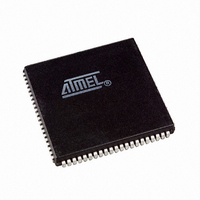
AT6002LV-4JC
Manufacturer Part Number
AT6002LV-4JC
Description
IC FPGA HP 4NS 6000 GATES 84PLCC
Manufacturer
Atmel
Series
AT6000(LV)r
Datasheet
1.AT6002-4JC.pdf
(28 pages)
Specifications of AT6002LV-4JC
Number Of Logic Elements/cells
1024
Number Of I /o
64
Number Of Gates
6000
Voltage - Supply
3.135 V ~ 3.465 V
Mounting Type
Surface Mount
Operating Temperature
0°C ~ 70°C
Package / Case
84-PLCC
Lead Free Status / RoHS Status
Contains lead / RoHS non-compliant
Number Of Labs/clbs
-
Total Ram Bits
-


AC Timing Characteristics – 3.3V Operation
Delays are based on fixed load. Loads for each type of device are described in the notes. Delays are in nanoseconds.
Worst case: V
Notes:
20
Cell Function
Wire
NAND
XOR
AND
MUX
D-Flip-flop
D-Flip-flop
D-Flip-flop
Bus Driver
Repeater
Column Clock
Column Reset
Clock Buffer
Reset Buffer
TTL Input
CMOS Input
Fast Output
Slow Output
Output Disable
Fast Enable
Slow Enable
Device
Cell
Bus
Column Clock
(6)
(6)
(4)
1. TTL buffer delays are measured from a V
2. CMOS buffer delays are measured from a V
3. Buffer delay is to a pad voltage of 1.5V with one output switching.
4. Max specifications are the average of mas t
5. Parameter based on characterization and simulation; not tested in production
6. Exact power calculation is available in an Atmel application note.
7. Load Definition: 1 = Load of one A or B input; 2 = Load of one L input; 3 = Constant Load; 4 = Load of 28 Clock Columns; 5
(1)
(5)
(5)
= Load of 28 Reset Columns; 6 = Tester Load of 50 pF.
(3)
(3)(5)
(5)
(3)
(5)
(2)
(3)(5)
AT6000(LV) Series
(6)
CC
(5)
= 3.0V to 3.6V. Temperature = 0 C to 70 C.
Parameter
t
t
t
t
t
t
t
t
t
t
t
t
t
t
t
t
t
t
t
t
t
PD
PD
PD
PD
PD
setup
hold
PD
PD
PD
PD
PD
PD
PD
PD
PD
PD
PD
PXZ
PXZ
PXZ
(max)
(max)
(max)
(max)
(max)
(max)
(max)
(max)
(max)
(max)
(max)
(max)
(max)
(max)
(max)
(max)
(min)
(max)
(max)
(max)
Cell Types
Wire, XWire, Half-adder, Flip-flop
Wire, XWire, Half-adder, Flip-flop, Repeater
Column Clock Driver
(min)
(4)
IH
of 1.5V at the pad to the internal V
PDLH
IH
GRES, A, EN
GCLK, A, ES
of 1/2 V
CLOCK PIN
RESET PIN
and t
A, B, L
A, B, L
A, B, L
A, B, L
A, B, L
From
CLK
CLK
A, B
L, E
L, E
I/O
I/O
A
A
A
L
L
L
L
PDHL
CC
at the apd to the internal V
.
I/O PIN
I/O PIN
I/O PIN
I/O PIN
I/O PIN
A, B, L
GRES
GCLK
RES
A, B
CLK
CLK
To
B
A
B
A
A
A
E
A
A
L
L
IH
Outputs
at A. The input buffer load is constant.
A, B
CLK
L
Definition
IH
at A. The input buffer load is constant.
Load
1
1
1
1
1
1
1
2
3
2
3
3
4
5
3
3
6
6
6
6
6
-
-
(7)
12.0
12.5
1.8
3.2
4.0
3.2
4.0
4.9
3.0
3.0
4.0
2.3
3.0
3.0
3.0
2.9
2.8
1.5
2.3
6.0
5.5
6.5
-4
0
2.3 µA/MHz
1.3 µA/MHz
20 µA/MHz
I
CC
(max)
Units
ns
ns
ns
ns
ns
ns
ns
ns
ns
ns
ns
ns
ns
ns
ns
ns
ns
ns
ns
ns
ns
ns
ns
Related parts for AT6002LV-4JC
Image
Part Number
Description
Manufacturer
Datasheet
Request
R

Part Number:
Description:
IC FPGA 4NS 100VQFP
Manufacturer:
Atmel
Datasheet:

Part Number:
Description:
DEV KIT FOR AVR/AVR32
Manufacturer:
Atmel
Datasheet:

Part Number:
Description:
INTERVAL AND WIPE/WASH WIPER CONTROL IC WITH DELAY
Manufacturer:
ATMEL Corporation
Datasheet:
Part Number:
Description:
Low-Voltage Voice-Switched IC for Hands-Free Operation
Manufacturer:
ATMEL Corporation
Datasheet:
Part Number:
Description:
MONOLITHIC INTEGRATED FEATUREPHONE CIRCUIT
Manufacturer:
ATMEL Corporation
Datasheet:
Part Number:
Description:
AM-FM Receiver IC U4255BM-M
Manufacturer:
ATMEL Corporation
Datasheet:
Part Number:
Description:
Monolithic Integrated Feature Phone Circuit
Manufacturer:
ATMEL Corporation
Datasheet:
Part Number:
Description:
Multistandard Video-IF and Quasi Parallel Sound Processing
Manufacturer:
ATMEL Corporation
Datasheet:
Part Number:
Description:
High-performance EE PLD
Manufacturer:
ATMEL Corporation
Datasheet:
Part Number:
Description:
8-bit Flash Microcontroller
Manufacturer:
ATMEL Corporation
Datasheet:
Part Number:
Description:
2-Wire Serial EEPROM
Manufacturer:
ATMEL Corporation
Datasheet: