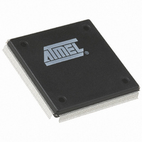
AT40K40LV-3EQC Atmel, AT40K40LV-3EQC Datasheet - Page 10

AT40K40LV-3EQC
Manufacturer Part Number
AT40K40LV-3EQC
Description
IC FPGA 3.3V 2304 CELL 240PQFP
Manufacturer
Atmel
Series
AT40K/KLVr
Datasheet
1.AT40K40LV-3BQC.pdf
(54 pages)
Specifications of AT40K40LV-3EQC
Number Of Logic Elements/cells
2304
Total Ram Bits
18432
Number Of I /o
193
Number Of Gates
50000
Voltage - Supply
3 V ~ 3.6 V
Mounting Type
Surface Mount
Operating Temperature
0°C ~ 70°C
Package / Case
240-BFQFP
Lead Free Status / RoHS Status
Contains lead / RoHS non-compliant
Number Of Labs/clbs
-
Other names
AT40K40LV3EQC
Reading and writing the 32 x 4 Dual-Port RAM are inde-
pendent of each other. Reading the 32 x 4 Dual-Port RAM
is completely asynchronous. Latches are transparent;
when Load is logic 1, data flows through; when Load is
logic 0, data is latched. Each bit in the 32 x 4 Dual-Port
RAM is also a transparent latch. The front-end latch and
the memory latch together form an edge-triggered flip flop.
When a Bit = 7 Nibble is (Write) addressed and LOAD is
Logic 1 and WE is logic 0, DATA flows through the bit.
Figure 8. RAM Logic
10
WRITE ADDR
READ ADDR
DATA IN
WE
5
5
4
AT40K
"1
Latch
Latch
Latch
Load
Load
Load
CLOCK
Read
Write
Write Enable
Data
RAM-Clear
Dual-Port
Clear
Load
32 x 4
RAM
When a nibble is not (Write) addressed or LOAD is logic 0
or WE is logic 1, DATA is latched in the nibble. The two
CLOCK muxes are controlled together; they both select
CLOCK or they both select “1”. CLOCK is obtained from
the clock for the sector-column immediately to the left and
immediately above the RAM block. Writing any value to the
RAM Clear Byte during configuration clears the RAM (see
Bit Map Spec).
"1
Data
"1
OE
4
DATA OUT


