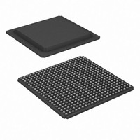
XC3S1600E-5FGG484C Xilinx Inc, XC3S1600E-5FGG484C Datasheet - Page 134

XC3S1600E-5FGG484C
Manufacturer Part Number
XC3S1600E-5FGG484C
Description
IC FPGA SPARTAN-3E 1600K 484FBGA
Manufacturer
Xilinx Inc
Series
Spartan™-3Er
Datasheet
1.XC3S100E-4VQG100C.pdf
(233 pages)
Specifications of XC3S1600E-5FGG484C
Number Of Logic Elements/cells
33192
Number Of Labs/clbs
3688
Total Ram Bits
663552
Number Of I /o
376
Number Of Gates
1600000
Voltage - Supply
1.14 V ~ 1.26 V
Mounting Type
Surface Mount
Operating Temperature
0°C ~ 85°C
Package / Case
484-BBGA
For Use With
HW-XA3S1600E-UNI-G - KIT DEVELOPMENT AUTOMOTIVE ECU
Lead Free Status / RoHS Status
Lead free / RoHS Compliant
Available stocks
Company
Part Number
Manufacturer
Quantity
Price
Company:
Part Number:
XC3S1600E-5FGG484C
Manufacturer:
XilinxInc
Quantity:
3 000
Company:
Part Number:
XC3S1600E-5FGG484C
Manufacturer:
Xilinx Inc
Quantity:
10 000
- Current page: 134 of 233
- Download datasheet (6Mb)
DC and Switching Characteristics
Timing Measurement Methodology
When measuring timing parameters at the programmable
I/Os, different signal standards call for different test condi-
tions.
The method for measuring Input timing is as follows: A sig-
nal that swings between a Low logic level of V
logic level of V
standards also require the application of a bias voltage to
the V
input-switching threshold. The measurement point of the
Input signal (V
and V
The Output test setup is shown in
voltage V
end of which is connected to the Output. For each standard,
R
mended for minimizing signal reflections. If the standard
does not ordinarily use terminations (e.g., LVCMOS,
LVTTL), then R
Table 95: Test Methods for Timing Measurement at I/Os
134
Single-Ended
LVTTL
LVCMOS33
LVCMOS25
LVCMOS18
LVCMOS15
LVCMOS12
PCI33_3
PCI66_3
HSTL_I_18
HSTL_III_18
SSTL18_I
SSTL2_I
Differential
LVDS_25
BLVDS_25
MINI_LVDS_25
LVPECL_25
RSDS_25
DIFF_HSTL_I_18
DIFF_HSTL_III_18
T
and V
Signal Standard
Table 95
H
(IOSTANDARD)
REF
.
T
T
is applied to the termination resistor R
pins of a given bank to properly set the
generally take on the standard values recom-
M
Rising
Falling
Rising
Falling
lists the conditions to use for each standard.
H
T
) is commonly located halfway between V
is set to 1MΩ to indicate an open connec-
is applied to the Input under test. Some
V
REF
1.25
0.9
1.1
0.9
-
-
-
-
-
-
-
-
-
-
-
-
-
-
-
Figure
(V)
73. A termination
V
V
V
V
V
V
V
V
V
V
V
ICM
ICM
ICM
REF
REF
REF
REF
REF
REF
ICM
ICM
Note 3
Note 3
V
L
Inputs
L
– 0.125
– 0.125
– 0.125
and a High
0
0
0
0
0
0
T
– 0.75
(V)
– 0.3
– 0.1
, the other
– 0.5
– 0.5
– 0.5
– 0.5
– 0.5
www.xilinx.com
L
V
V
V
V
V
V
V
V
V
V
V
ICM
ICM
ICM
REF
REF
REF
REF
REF
REF
ICM
ICM
Note 3
Note 3
V
tion, and V
(V
H
3.3
3.3
2.5
1.8
1.5
1.2
+ 0.125
+ 0.125
+ 0.125
+ 0.75
(V)
+ 0.3
+ 0.1
+ 0.5
+ 0.5
+ 0.5
+ 0.5
+ 0.5
M
) that was used at the Input is also used at the Output.
Notes:
1.
FPGA Output
T
is set to zero. The same measurement point
Figure 73: Output Test Setup
The names shown in parentheses are
used in the IBIS file.
R
1M
1M
1M
1M
1M
1M
1M
1M
T
25
25
25
25
50
50
50
50
50
50
50
50
50
(Ω)
Outputs
V
T
(V
REF
R
DS312-3 (v3.8) August 26, 2009
C
T
L
V
1.25
(R
T
3.3
3.3
0.9
1.8
0.9
1.2
1.2
1.2
0.9
1.8
(C
)
V
0
0
0
0
0
0
0
0
0
0
(V)
M
REF
REF
(V
ds312-3_04_090105
Product Specification
)
MEAS
)
)
Inputs and
Outputs
V
V
V
V
V
V
V
V
V
V
V
V
1.65
1.25
0.75
0.94
2.03
0.94
2.03
M
1.4
0.9
0.6
REF
REF
REF
REF
ICM
ICM
ICM
ICM
ICM
ICM
ICM
(V)
R
Related parts for XC3S1600E-5FGG484C
Image
Part Number
Description
Manufacturer
Datasheet
Request
R

Part Number:
Description:
IC SPARTAN-3E FPGA 1600K 320-FBG
Manufacturer:
Xilinx Inc
Datasheet:

Part Number:
Description:
IC SPARTAN-3E FPGA 1600K 400FBGA
Manufacturer:
Xilinx Inc
Datasheet:

Part Number:
Description:
IC FPGA SPARTAN-3E 1600K 320FBGA
Manufacturer:
Xilinx Inc
Datasheet:

Part Number:
Description:
IC FPGA SPARTAN-3E 1600K 320FBGA
Manufacturer:
Xilinx Inc
Datasheet:

Part Number:
Description:
IC FPGA SPARTAN-3E 1600K 400FBGA
Manufacturer:
Xilinx Inc
Datasheet:

Part Number:
Description:
IC FPGA SPARTAN 3E 320FBGA
Manufacturer:
Xilinx Inc
Datasheet:

Part Number:
Description:
IC FPGA SPARTAN 3E 400FBGA
Manufacturer:
Xilinx Inc
Datasheet:

Part Number:
Description:
IC FPGA SPARTAN 3E 484FBGA
Manufacturer:
Xilinx Inc
Datasheet:

Part Number:
Description:
FPGA, SPARTAN-3E, 1600K GATES, 484FBGA
Manufacturer:
Xilinx Inc
Datasheet:

Part Number:
Description:
PROGRAMMABLE MICROCHIP
Manufacturer:
Xilinx Inc
Datasheet:

Part Number:
Description:
FPGA Spartan®-3E Family 1.6M Gates 33192 Cells 572MHz 90nm (CMOS) Technology 1.2V 484-Pin FBGA
Manufacturer:
Xilinx Inc
Datasheet:

Part Number:
Description:
FPGA Spartan®-3E Family 1.6M Gates 33192 Cells 657MHz 90nm (CMOS) Technology 1.2V 400-Pin FBGA
Manufacturer:
Xilinx Inc
Datasheet:

Part Number:
Description:
FPGA Spartan®-3E Family 1.6M Gates 33192 Cells 657MHz 90nm (CMOS) Technology 1.2V 400-Pin FBGA
Manufacturer:
Xilinx Inc
Datasheet:

Part Number:
Description:
FPGA Spartan®-3E Family 1.6M Gates 33192 Cells 572MHz 90nm (CMOS) Technology 1.2V 320-Pin FBGA
Manufacturer:
Xilinx Inc
Datasheet:

Part Number:
Description:
IC CPLD .8K 36MCELL 44-VQFP
Manufacturer:
Xilinx Inc
Datasheet:


