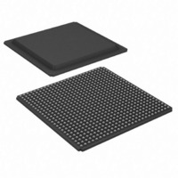
XC3S1000-4FGG676I Xilinx Inc, XC3S1000-4FGG676I Datasheet - Page 102

XC3S1000-4FGG676I
Manufacturer Part Number
XC3S1000-4FGG676I
Description
SPARTAN-3A FPGA 1M STD 676-FBGA
Manufacturer
Xilinx Inc
Series
Spartan™-3r
Datasheet
1.XC3S50-4VQG100C.pdf
(217 pages)
Specifications of XC3S1000-4FGG676I
Number Of Logic Elements/cells
17280
Number Of Labs/clbs
1920
Total Ram Bits
442368
Number Of I /o
391
Number Of Gates
1000000
Voltage - Supply
1.14 V ~ 1.26 V
Mounting Type
Surface Mount
Operating Temperature
-40°C ~ 100°C
Package / Case
676-BBGA
For Use With
122-1502 - KIT STARTER SPARTAN-3 PCI-E
Lead Free Status / RoHS Status
Lead free / RoHS Compliant
Available stocks
Company
Part Number
Manufacturer
Quantity
Price
Company:
Part Number:
XC3S1000-4FGG676I
Manufacturer:
XilinxInc
Quantity:
3 000
Company:
Part Number:
XC3S1000-4FGG676I
Manufacturer:
Xilinx Inc
Quantity:
10 000
Spartan-3 FPGA Family: Pinout Descriptions
Table 69: Spartan-3 FPGA Pin Definitions (Continued)
102
IO_Lxxy_#/INIT_B
DCI: Digitally Controlled Impedance reference resistor input pins
IO_Lxxy_#/VRN_# or
IO/VRN_#
IO_Lxxy_#/VRP_# or
IO/VRP_#
GCLK: Global clock buffer inputs
IO_Lxxy_#/GCLK0,
IO_Lxxy_#/GCLK1,
IO_Lxxy_#/GCLK2,
IO_Lxxy_#/GCLK3,
IO_Lxxy_#/GCLK4,
IO_Lxxy_#/GCLK5,
IO_Lxxy_#/GCLK6,
IO_Lxxy_#/GCLK7
VREF: I/O bank input reference voltage pins
IO_Lxxy_#/VREF_#
or
IO/VREF_#
CONFIG: Dedicated configuration pins (pull-up resistor to VCCAUX always active during configuration, regardless of
HSWAP_EN pin)
CCLK
PROG_B
Pin Name
Bidirectional (open-drain)
during configuration
User I/O after configuration
Input when using DCI
Otherwise, same as I/O
Input when using DCI
Otherwise, same as I/O
Input if connected to global
clock buffers
Otherwise, same as I/O
Voltage supply input when
VREF pins are used within a
bank.
Otherwise, same as I/O
Input in Slave configuration
modes
Output in Master
configuration modes
Input
Direction
www.xilinx.com
Initializing Configuration Memory/Detected Configuration Error:
When Low, this pin indicates that configuration memory is being
cleared. When held Low, this pin delays the start of configuration.
After this pin is released or configuration memory is cleared, the
pin goes High. During configuration, a Low on this output indicates
that a configuration data error occurred. This pin always has an
internal pull-up resistor to VCCO_4 or VCCO_BOTTOM during
configuration, regardless of the HSWAP_EN pin. This pin
becomes a user I/O after configuration.
DCI Reference Resistor for NMOS I/O Transistor (per bank):
If using DCI, a 1% precision impedance-matching resistor is
connected between this pin and the VCCO supply for this bank.
Otherwise, this pin is a user I/O.
DCI Reference Resistor for PMOS I/O Transistor (per bank):
If using DCI, a 1% precision impedance-matching resistor is
connected between this pin and the ground supply. Otherwise, this
pin is a user I/O.
Global Buffer Input:
Direct input to a low-skew global clock buffer. If not connected to a
global clock buffer, this pin is a user I/O.
Input Buffer Reference Voltage for Special I/O Standards (per
bank):
If required to support special I/O standards, all the VREF pins
within a bank connect to a input threshold voltage source.
If not used as input reference voltage pins, these pins are available
as individual user-I/O pins.
Configuration Clock:
The configuration clock signal synchronizes configuration data.
This pin has an internal pull-up resistor to VCCAUX during
configuration.
Program/Configure Device:
Active Low asynchronous reset to configuration logic. Asserting
PROG_B Low for an extended period delays the configuration
process. This pin has an internal pull-up resistor to VCCAUX
during configuration.
Description
DS099-4 (v2.5) December 4, 2009
Product Specification
R


