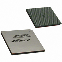
EP2SGX90FF1508C3N Altera, EP2SGX90FF1508C3N Datasheet - Page 154

EP2SGX90FF1508C3N
Manufacturer Part Number
EP2SGX90FF1508C3N
Description
IC STRATIX II GX 90K 1508-FBGA
Manufacturer
Altera
Series
Stratix® II GXr
Datasheet
1.EP2SGX90FF1508C3N.pdf
(314 pages)
Specifications of EP2SGX90FF1508C3N
Number Of Logic Elements/cells
90960
Number Of Labs/clbs
4548
Total Ram Bits
4520448
Number Of I /o
650
Voltage - Supply
1.15 V ~ 1.25 V
Mounting Type
Surface Mount
Operating Temperature
0°C ~ 70°C
Package / Case
1508-FBGA
For Use With
544-1725 - PCIE KIT W/S II GX EP2SGX90N544-1724 - SI KIT W/SII GX EP2SGX90N544-1702 - VIDEO KIT W/SII GX EP2SGX90N
Lead Free Status / RoHS Status
Lead free / RoHS Compliant
Number Of Gates
-
Other names
544-1772
EP2SGX90FF40C3N
EP2SGX90FF40C3NES
EP2SGX90FF40C3N
EP2SGX90FF40C3NES
Available stocks
Company
Part Number
Manufacturer
Quantity
Price
Company:
Part Number:
EP2SGX90FF1508C3N
Manufacturer:
ALTERA30
Quantity:
121
- Current page: 154 of 314
- Download datasheet (4Mb)
Document Revision History
2–146
Stratix II GX Device Handbook, Volume 1
Table 2–42. Document Revision History (Part 4 of 6)
Document
Date and
Version
Updated:
●
●
●
●
●
●
●
●
●
●
●
●
●
●
●
●
●
●
●
●
Updated bulleted lists at the beginning of the
“Transceivers” section.
Added reference to the “Transmit Buffer”
section.
Deleted the Programmable V
“Programmable Output Driver” section.
Data Width” heading in Table 2–14.
Deleted “Global & Regional Clock
Connections from Right Side Clock Pins &
Fast PLL Outputs” table.
Updated notes to Tables 2–29 and 2–37.
Updated notes to Figures 2–72, 2–73 and
2–74.
Updated bulleted list in the “Advanced I/O
Standard Support” section.
Changed “PLD Interface” heading to “Parallel
“Transmitter PLLs”
“Transmitter Phase Compensation FIFO
Buffer”
“8B/10B Encoder”
“Byte Serializer”
“Programmable Output Driver”
“Receiver PLL & CRU”
“Programmable Pre-Emphasis”
“Receiver Input Buffer”
“Control and Status Signals”
“Programmable Run Length Violation”
“Channel Aligner”
“Basic Mode”
“Byte Ordering Block”
“Receiver Phase Compensation FIFO
Buffer”
“Loopback Modes”
“Serial Loopback”
“Parallel Loopback”
“Regional Clock Network”
“MultiVolt I/O Interface”
“High-Speed Differential I/O with DPA
Support”
Changes Made
OD
table from the
Summary of Changes
Altera Corporation
October 2007
Related parts for EP2SGX90FF1508C3N
Image
Part Number
Description
Manufacturer
Datasheet
Request
R

Part Number:
Description:
CYCLONE II STARTER KIT EP2C20N
Manufacturer:
Altera
Datasheet:

Part Number:
Description:
CPLD, EP610 Family, ECMOS Process, 300 Gates, 16 Macro Cells, 16 Reg., 16 User I/Os, 5V Supply, 35 Speed Grade, 24DIP
Manufacturer:
Altera Corporation
Datasheet:

Part Number:
Description:
CPLD, EP610 Family, ECMOS Process, 300 Gates, 16 Macro Cells, 16 Reg., 16 User I/Os, 5V Supply, 15 Speed Grade, 24DIP
Manufacturer:
Altera Corporation
Datasheet:

Part Number:
Description:
Manufacturer:
Altera Corporation
Datasheet:

Part Number:
Description:
CPLD, EP610 Family, ECMOS Process, 300 Gates, 16 Macro Cells, 16 Reg., 16 User I/Os, 5V Supply, 30 Speed Grade, 24DIP
Manufacturer:
Altera Corporation
Datasheet:

Part Number:
Description:
High-performance, low-power erasable programmable logic devices with 8 macrocells, 10ns
Manufacturer:
Altera Corporation
Datasheet:

Part Number:
Description:
High-performance, low-power erasable programmable logic devices with 8 macrocells, 7ns
Manufacturer:
Altera Corporation
Datasheet:

Part Number:
Description:
Classic EPLD
Manufacturer:
Altera Corporation
Datasheet:

Part Number:
Description:
High-performance, low-power erasable programmable logic devices with 8 macrocells, 10ns
Manufacturer:
Altera Corporation
Datasheet:

Part Number:
Description:
Manufacturer:
Altera Corporation
Datasheet:

Part Number:
Description:
Manufacturer:
Altera Corporation
Datasheet:

Part Number:
Description:
Manufacturer:
Altera Corporation
Datasheet:

Part Number:
Description:
CPLD, EP610 Family, ECMOS Process, 300 Gates, 16 Macro Cells, 16 Reg., 16 User I/Os, 5V Supply, 25 Speed Grade, 24DIP
Manufacturer:
Altera Corporation
Datasheet:


