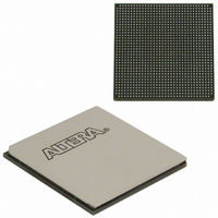
EP2SGX90EF1152C5ES Altera, EP2SGX90EF1152C5ES Datasheet - Page 3

EP2SGX90EF1152C5ES
Manufacturer Part Number
EP2SGX90EF1152C5ES
Description
IC STRATIX II GX 90K 1152-FBGA
Manufacturer
Altera
Series
Stratix® II GXr
Datasheet
1.EP2SGX30DF780C5.pdf
(316 pages)
Specifications of EP2SGX90EF1152C5ES
Number Of Logic Elements/cells
90960
Number Of Labs/clbs
4548
Total Ram Bits
4520448
Number Of I /o
558
Voltage - Supply
1.15 V ~ 1.25 V
Mounting Type
Surface Mount
Operating Temperature
0°C ~ 70°C
Package / Case
1152-FBGA
For Use With
544-1725 - PCIE KIT W/S II GX EP2SGX90N544-1724 - SI KIT W/SII GX EP2SGX90N544-1702 - VIDEO KIT W/SII GX EP2SGX90N
Lead Free Status / RoHS Status
Contains lead / RoHS non-compliant
Number Of Gates
-
Other names
544-1765
Available stocks
Company
Part Number
Manufacturer
Quantity
Price
- Current page: 3 of 316
- Download datasheet (2Mb)
Features
Altera Corporation
October 2007
SIIGX51001-1.6
The Stratix
to combine high-speed serial transceivers with a scalable,
high-performance logic array. Stratix II GX devices include 4 to 20
high-speed transceiver channels, each incorporating clock and data
recovery unit (CRU) technology and embedded SERDES capability at
data rates of up to 6.375 gigabits per second (Gbps). The transceivers are
grouped into four-channel transceiver blocks and are designed for low
power consumption and small die size. The Stratix II GX FPGA
technology is built upon the Stratix II architecture and offers a 1.2-V logic
array with unmatched performance, flexibility, and time-to-market
capabilities. This scalable, high-performance architecture makes
Stratix II GX devices ideal for high-speed backplane interface,
chip-to-chip, and communications protocol-bridging applications.
This section lists the Stratix II GX device features.
■
Main device features:
●
●
●
●
●
●
●
●
TriMatrix memory consisting of three RAM block sizes to
implement true dual-port memory and first-in first-out (FIFO)
buffers with performance up to 550 MHz
Up to 16 global clock networks with up to 32 regional clock
networks per device region
High-speed DSP blocks provide dedicated implementation of
multipliers (at up to 450 MHz), multiply-accumulate functions,
and finite impulse response (FIR) filters
Up to four enhanced PLLs per device provide spread spectrum,
programmable bandwidth, clock switch-over, real-time PLL
reconfiguration, and advanced multiplication and phase
shifting
Support for numerous single-ended and differential I/O
standards
High-speed source-synchronous differential I/O support on up
to 71 channels
Support for source-synchronous bus standards, including SPI-4
Phase 2 (POS-PHY Level 4), SFI-4.1, XSBI, UTOPIA IV, NPSI,
and CSIX-L1
Support for high-speed external memory, including quad data
rate (QDR and QDRII) SRAM, double data rate (DDR and
DDR2) SDRAM, and single data rate (SDR) SDRAM
®
II GX family of devices is Altera’s third generation of FPGAs
1. Introduction
1–1
Related parts for EP2SGX90EF1152C5ES
Image
Part Number
Description
Manufacturer
Datasheet
Request
R

Part Number:
Description:
CYCLONE II STARTER KIT EP2C20N
Manufacturer:
Altera
Datasheet:

Part Number:
Description:
CPLD, EP610 Family, ECMOS Process, 300 Gates, 16 Macro Cells, 16 Reg., 16 User I/Os, 5V Supply, 35 Speed Grade, 24DIP
Manufacturer:
Altera Corporation
Datasheet:

Part Number:
Description:
CPLD, EP610 Family, ECMOS Process, 300 Gates, 16 Macro Cells, 16 Reg., 16 User I/Os, 5V Supply, 15 Speed Grade, 24DIP
Manufacturer:
Altera Corporation
Datasheet:

Part Number:
Description:
Manufacturer:
Altera Corporation
Datasheet:

Part Number:
Description:
CPLD, EP610 Family, ECMOS Process, 300 Gates, 16 Macro Cells, 16 Reg., 16 User I/Os, 5V Supply, 30 Speed Grade, 24DIP
Manufacturer:
Altera Corporation
Datasheet:

Part Number:
Description:
High-performance, low-power erasable programmable logic devices with 8 macrocells, 10ns
Manufacturer:
Altera Corporation
Datasheet:

Part Number:
Description:
High-performance, low-power erasable programmable logic devices with 8 macrocells, 7ns
Manufacturer:
Altera Corporation
Datasheet:

Part Number:
Description:
Classic EPLD
Manufacturer:
Altera Corporation
Datasheet:

Part Number:
Description:
High-performance, low-power erasable programmable logic devices with 8 macrocells, 10ns
Manufacturer:
Altera Corporation
Datasheet:

Part Number:
Description:
Manufacturer:
Altera Corporation
Datasheet:

Part Number:
Description:
Manufacturer:
Altera Corporation
Datasheet:

Part Number:
Description:
Manufacturer:
Altera Corporation
Datasheet:

Part Number:
Description:
CPLD, EP610 Family, ECMOS Process, 300 Gates, 16 Macro Cells, 16 Reg., 16 User I/Os, 5V Supply, 25 Speed Grade, 24DIP
Manufacturer:
Altera Corporation
Datasheet:


