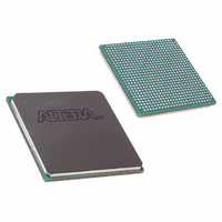
EP2S60F672I4 Altera, EP2S60F672I4 Datasheet - Page 90

EP2S60F672I4
Manufacturer Part Number
EP2S60F672I4
Description
IC STRATIX II FPGA 60K 672-FBGA
Manufacturer
Altera
Series
Stratix® IIr
Datasheet
1.EP2S15F484I4N.pdf
(238 pages)
Specifications of EP2S60F672I4
Number Of Logic Elements/cells
60440
Number Of Labs/clbs
3022
Total Ram Bits
2544192
Number Of I /o
492
Voltage - Supply
1.15 V ~ 1.25 V
Mounting Type
Surface Mount
Operating Temperature
-40°C ~ 100°C
Package / Case
672-FBGA
Family Name
Stratix II
Number Of Logic Blocks/elements
60440
# I/os (max)
492
Frequency (max)
711.24MHz
Process Technology
90nm (CMOS)
Operating Supply Voltage (typ)
1.2V
Logic Cells
60440
Ram Bits
2544192
Operating Supply Voltage (min)
1.15V
Operating Supply Voltage (max)
1.25V
Operating Temp Range
-40C to 100C
Operating Temperature Classification
Industrial
Mounting
Surface Mount
Pin Count
672
Package Type
FC-FBGA
For Use With
544-1700 - DSP KIT W/STRATIX II EP2S60N544-1697 - NIOS II KIT W/STRATIX II EP2S60N
Lead Free Status / RoHS Status
Contains lead / RoHS non-compliant
Number Of Gates
-
Lead Free Status / Rohs Status
Not Compliant
Other names
544-1915
EP2S60F672I4
EP2S60F672I4
Available stocks
Company
Part Number
Manufacturer
Quantity
Price
Company:
Part Number:
EP2S60F672I4N
Manufacturer:
ALTERA
Quantity:
201
Company:
Part Number:
EP2S60F672I4N
Manufacturer:
ALTERA
Quantity:
400
Part Number:
EP2S60F672I4N
Manufacturer:
ALTERA/阿尔特拉
Quantity:
20 000
I/O Structure
2–82
Stratix II Device Handbook, Volume 1
Notes to
(1)
EP2S90
EP2S130 780-pin FineLine BGA
EP2S180 1,020-pin FineLine BGA
Table 2–14. DQS & DQ Bus Mode Support (Part 2 of 2)
Device
Check the pin table for each DQS/DQ group in the different modes.
Table
484-pin Hybrid FineLine BGA
780-pin FineLine BGA
1,020-pin FineLine BGA
1,508-pin FineLine BGA
1,020-pin FineLine BGA
1,508-pin FineLine BGA
1,508-pin FineLine BGA
2–14:
Package
A compensated delay element on each DQS pin automatically aligns
input DQS synchronization signals with the data window of their
corresponding DQ data signals. The DQS signals drive a local DQS bus in
the top and bottom I/O banks. This DQS bus is an additional resource to
the I/O clocks and is used to clock DQ input registers with the DQS
signal.
The Stratix II device has two phase-shifting reference circuits, one on the
top and one on the bottom of the device. The circuit on the top controls
the compensated delay elements for all DQS pins on the top. The circuit
on the bottom controls the compensated delay elements for all DQS pins
on the bottom.
Each phase-shifting reference circuit is driven by a system reference clock,
which must have the same frequency as the DQS signal. Clock pins
CLK[15..12]p feed the phase circuitry on the top of the device and
clock pins CLK[7..4]p feed the phase circuitry on the bottom of the
device. In addition, PLL clock outputs can also feed the phase-shifting
reference circuits.
Figure 2–56
DQS delay shift on the top of the device. This same circuit is duplicated
on the bottom of the device.
illustrates the phase-shift reference circuit control of each
Number of
×4 Groups
18
36
36
18
36
36
36
36
8
×8/×9 Groups
Number of
Note (1)
18
18
18
18
18
18
4
8
8
×16/×18 Groups
Number of
0
4
8
8
4
8
8
8
8
Altera Corporation
×32/×36 Groups
Number of
May 2007
0
0
4
4
0
4
4
4
4


