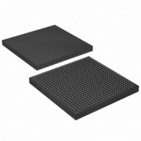
EP1S20F672C6 Altera, EP1S20F672C6 Datasheet - Page 204

EP1S20F672C6
Manufacturer Part Number
EP1S20F672C6
Description
IC STRATIX FPGA 20K LE 672-FBGA
Manufacturer
Altera
Series
Stratix®r
Datasheet
1.EP1S10F780C7.pdf
(276 pages)
Specifications of EP1S20F672C6
Number Of Logic Elements/cells
18460
Number Of Labs/clbs
1846
Total Ram Bits
1669248
Number Of I /o
426
Voltage - Supply
1.425 V ~ 1.575 V
Mounting Type
Surface Mount
Operating Temperature
0°C ~ 85°C
Package / Case
672-FBGA
Lead Free Status / RoHS Status
Contains lead / RoHS non-compliant
Number Of Gates
-
Other names
544-1853
EP1S20F672C6
EP1S20F672C6
Available stocks
Company
Part Number
Manufacturer
Quantity
Price
Company:
Part Number:
EP1S20F672C6
Manufacturer:
ALTERA
Quantity:
528
Part Number:
EP1S20F672C6N
Manufacturer:
ALTERA/阿尔特拉
Quantity:
20 000
- Current page: 204 of 276
- Download datasheet (4Mb)
Timing Model
4–34
Stratix Device Handbook, Volume 1
Table 4–52
regional clock networks.
Table 4–53
regional clock networks.
Notes to
(1)
(2)
t
t
t
t
t
t
t
t
t
t
t
INSU
INH
OUTCO
XZ
ZX
INSU
INH
OUTCO
INSUPLL
INHPLL
OUTCOPLL
Table 4–52. Stratix Fast Regional Clock External I/O Timing Parameters
Table 4–53. Stratix Regional Clock External I/O Timing Parameters (Part 1
of 2)
Symbol
Symbol
Notes
These timing parameters are sample-tested only.
These timing parameters are for column and row IOE pins. You should use the
Quartus II software to verify the external timing for any pin.
Notes
(1),
Table
shows the external I/O timing parameters when using fast
shows the external I/O timing parameters when using
Setup time for input or bidirectional pin using IOE input register with
fast regional clock fed by
Hold time for input or bidirectional pin using IOE input register with
fast regional clock fed by
Clock-to-output delay output or bidirectional pin using IOE output
register with fast regional clock fed by
Synchronous IOE output enable register to output pin disable delay
using fast regional clock fed by
Synchronous IOE output enable register to output pin enable delay
using fast regional clock fed by
(2)
Setup time for input or bidirectional pin using IOE input register with
regional clock fed by
Hold time for input or bidirectional pin using IOE input register with
regional clock fed by
Clock-to-output delay output or bidirectional pin using IOE output
register with regional clock fed by
Setup time for input or bidirectional pin using IOE input register with
regional clock fed by Enhanced PLL with default phase setting
Hold time for input or bidirectional pin using IOE input register with
regional clock fed by Enhanced PLL with default phase setting
Clock-to-output delay output or bidirectional pin using IOE output
register with regional clock Enhanced PLL with default phase setting
(1),
4–52:
(2)
CLK
CLK
FCLK
FCLK
pin
pin
Parameter
Parameter
FCLK
pin
pin
FCLK
CLK
FCLK
pin
pin
pin
pin
Altera Corporation
January 2006
Related parts for EP1S20F672C6
Image
Part Number
Description
Manufacturer
Datasheet
Request
R

Part Number:
Description:
CYCLONE II STARTER KIT EP2C20N
Manufacturer:
Altera
Datasheet:

Part Number:
Description:
CPLD, EP610 Family, ECMOS Process, 300 Gates, 16 Macro Cells, 16 Reg., 16 User I/Os, 5V Supply, 35 Speed Grade, 24DIP
Manufacturer:
Altera Corporation
Datasheet:

Part Number:
Description:
CPLD, EP610 Family, ECMOS Process, 300 Gates, 16 Macro Cells, 16 Reg., 16 User I/Os, 5V Supply, 15 Speed Grade, 24DIP
Manufacturer:
Altera Corporation
Datasheet:

Part Number:
Description:
Manufacturer:
Altera Corporation
Datasheet:

Part Number:
Description:
CPLD, EP610 Family, ECMOS Process, 300 Gates, 16 Macro Cells, 16 Reg., 16 User I/Os, 5V Supply, 30 Speed Grade, 24DIP
Manufacturer:
Altera Corporation
Datasheet:

Part Number:
Description:
High-performance, low-power erasable programmable logic devices with 8 macrocells, 10ns
Manufacturer:
Altera Corporation
Datasheet:

Part Number:
Description:
High-performance, low-power erasable programmable logic devices with 8 macrocells, 7ns
Manufacturer:
Altera Corporation
Datasheet:

Part Number:
Description:
Classic EPLD
Manufacturer:
Altera Corporation
Datasheet:

Part Number:
Description:
High-performance, low-power erasable programmable logic devices with 8 macrocells, 10ns
Manufacturer:
Altera Corporation
Datasheet:

Part Number:
Description:
Manufacturer:
Altera Corporation
Datasheet:

Part Number:
Description:
Manufacturer:
Altera Corporation
Datasheet:

Part Number:
Description:
Manufacturer:
Altera Corporation
Datasheet:

Part Number:
Description:
CPLD, EP610 Family, ECMOS Process, 300 Gates, 16 Macro Cells, 16 Reg., 16 User I/Os, 5V Supply, 25 Speed Grade, 24DIP
Manufacturer:
Altera Corporation
Datasheet:


