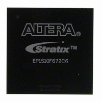
EP1S10F672C6 Altera, EP1S10F672C6 Datasheet - Page 133

EP1S10F672C6
Manufacturer Part Number
EP1S10F672C6
Description
IC STRATIX FPGA 10K LE 672-FBGA
Manufacturer
Altera
Series
Stratix®r
Datasheet
1.EP1S10F780C7.pdf
(276 pages)
Specifications of EP1S10F672C6
Number Of Logic Elements/cells
10570
Number Of Labs/clbs
1057
Total Ram Bits
920448
Number Of I /o
345
Voltage - Supply
1.425 V ~ 1.575 V
Mounting Type
Surface Mount
Operating Temperature
0°C ~ 85°C
Package / Case
672-FBGA
Lead Free Status / RoHS Status
Contains lead / RoHS non-compliant
Number Of Gates
-
Other names
544-1108
Available stocks
Company
Part Number
Manufacturer
Quantity
Price
Company:
Part Number:
EP1S10F672C6
Manufacturer:
KAWASAKI
Quantity:
1 200
Company:
Part Number:
EP1S10F672C6
Manufacturer:
ALTERA
Quantity:
3 000
Company:
Part Number:
EP1S10F672C6N
Manufacturer:
ALTERA
Quantity:
3 000
- Current page: 133 of 276
- Download datasheet (4Mb)
Figure 2–69. Simplified Diagram of the DQS Phase-Shift Circuitry
Altera Corporation
July 2005
Reference
Clock
Input
shift by the same degree amount. For example, all 10 DQS pins on the top
of the device can be shifted by 90° and all 10 DQS pins on the bottom of
the device can be shifted by 72°. The reference circuits require a maximum
of 256 system reference clock cycles to set the correct phase on the DQS
delay elements.
control of each DQS delay shift on the top of the device. This same circuit
is duplicated on the bottom of the device.
See the External Memory Interfaces chapter in the Stratix Device Handbook,
Volume 2 for more information on external memory interfaces.
Programmable Drive Strength
The output buffer for each Stratix device I/O pin has a programmable
drive strength control for certain I/O standards. The LVTTL and
LVCMOS standard has several levels of drive strength that the user can
control. SSTL-3 Class I and II, SSTL-2 Class I and II, HSTL Class I and II,
and 3.3-V GTL+ support a minimum setting, the lowest drive strength
that guarantees the I
provides signal slew rate control to reduce system noise and signal
overshoot.
Comparator
Phase
Delay Chains
Figure 2–69
OH
/I
OL
Up/Down
of the standard. Using minimum settings
Counter
illustrates the phase-shift reference circuit
6
Stratix Device Handbook, Volume 1
Control Signals
to DQS Pins
Stratix Architecture
2–119
Related parts for EP1S10F672C6
Image
Part Number
Description
Manufacturer
Datasheet
Request
R

Part Number:
Description:
CYCLONE II STARTER KIT EP2C20N
Manufacturer:
Altera
Datasheet:

Part Number:
Description:
CPLD, EP610 Family, ECMOS Process, 300 Gates, 16 Macro Cells, 16 Reg., 16 User I/Os, 5V Supply, 35 Speed Grade, 24DIP
Manufacturer:
Altera Corporation
Datasheet:

Part Number:
Description:
CPLD, EP610 Family, ECMOS Process, 300 Gates, 16 Macro Cells, 16 Reg., 16 User I/Os, 5V Supply, 15 Speed Grade, 24DIP
Manufacturer:
Altera Corporation
Datasheet:

Part Number:
Description:
Manufacturer:
Altera Corporation
Datasheet:

Part Number:
Description:
CPLD, EP610 Family, ECMOS Process, 300 Gates, 16 Macro Cells, 16 Reg., 16 User I/Os, 5V Supply, 30 Speed Grade, 24DIP
Manufacturer:
Altera Corporation
Datasheet:

Part Number:
Description:
High-performance, low-power erasable programmable logic devices with 8 macrocells, 10ns
Manufacturer:
Altera Corporation
Datasheet:

Part Number:
Description:
High-performance, low-power erasable programmable logic devices with 8 macrocells, 7ns
Manufacturer:
Altera Corporation
Datasheet:

Part Number:
Description:
Classic EPLD
Manufacturer:
Altera Corporation
Datasheet:

Part Number:
Description:
High-performance, low-power erasable programmable logic devices with 8 macrocells, 10ns
Manufacturer:
Altera Corporation
Datasheet:

Part Number:
Description:
Manufacturer:
Altera Corporation
Datasheet:

Part Number:
Description:
Manufacturer:
Altera Corporation
Datasheet:

Part Number:
Description:
Manufacturer:
Altera Corporation
Datasheet:

Part Number:
Description:
CPLD, EP610 Family, ECMOS Process, 300 Gates, 16 Macro Cells, 16 Reg., 16 User I/Os, 5V Supply, 25 Speed Grade, 24DIP
Manufacturer:
Altera Corporation
Datasheet:


