EP1C4F324C6N Altera, EP1C4F324C6N Datasheet - Page 59
EP1C4F324C6N
Manufacturer Part Number
EP1C4F324C6N
Description
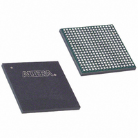
IC CYCLONE FPGA 4K LE 324-FBGA
Manufacturer
Altera
Series
Cyclone®r
Datasheet
1.EP1C3T144C8.pdf
(106 pages)
Specifications of EP1C4F324C6N
Number Of Logic Elements/cells
4000
Number Of Labs/clbs
400
Total Ram Bits
78336
Number Of I /o
249
Voltage - Supply
1.425 V ~ 1.575 V
Mounting Type
Surface Mount
Operating Temperature
0°C ~ 85°C
Package / Case
324-FBGA
Family Name
Cyclone®
Number Of Logic Blocks/elements
4000
# I/os (max)
249
Frequency (max)
405.2MHz
Process Technology
0.13um (CMOS)
Operating Supply Voltage (typ)
1.5V
Logic Cells
4000
Ram Bits
78336
Operating Supply Voltage (min)
1.425V
Operating Supply Voltage (max)
1.575V
Operating Temp Range
0C to 85C
Operating Temperature Classification
Commercial
Mounting
Surface Mount
Pin Count
324
Package Type
FBGA
Lead Free Status / RoHS Status
Lead free / RoHS Compliant
Number Of Gates
-
Lead Free Status / Rohs Status
Compliant
Other names
544-1803
EP1C4F324C6N
EP1C4F324C6N
Available stocks
Company
Part Number
Manufacturer
Quantity
Price
Company:

Part Number:
EP1C4F324C6N
Manufacturer:
ALTERA
Quantity:
5 510
Company:
Part Number:
EP1C4F324C6N
Manufacturer:
ALTERA
Quantity:
250
Part Number:
EP1C4F324C6N
Manufacturer:
ALTERA
Quantity:
20 000


Figure 2–35. Cyclone I/O Banks
Notes to
(1)
(2)
Altera Corporation
May 2008
Also Supports
Figure 2–35
Figure 2–35
the 3.3-V PCI
I/O Standard
I/O Bank 1
Figure
I/O Bank 1
2–35:
is a top view of the silicon die.
is a graphic representation only. Refer to the pin list and the Quartus II software for exact pin locations.
and DM pins to support a DDR SDRAM or FCRAM interface. I/O bank 1
can also support a DDR SDRAM or FCRAM interface, however, the
configuration input pins in I/O bank 1 must operate at 2.5 V. I/O bank 3
can also support a DDR SDRAM or FCRAM interface, however, all the
JTAG pins in I/O bank 3 must operate at 2.5 V.
Each I/O bank has its own VCCIO pins. A single device can support 1.5-V,
1.8-V, 2.5-V, and 3.3-V interfaces; each individual bank can support a
different standard with different I/O voltages. Each bank also has
dual-purpose VREF pins to support any one of the voltage-referenced
standards (e.g., SSTL-3) independently. If an I/O bank does not use
voltage-referenced standards, the V
Notes
(1),
All I/O Banks Support
■
■
■
■
■
■
■
■
(2)
3.3-V LVTTL/LVCMOS
2.5-V LVTTL/LVCMOS
1.8-V LVTTL/LVCMOS
1.5-V LVCMOS
LVDS
RSDS
SSTL-2 Class I and II
SSTL-3 Class I and II
I/O Bank 2
I/O Bank 4
Power Bus
Individual
REF
pins are available as user I/O pins.
I/O Bank 3
I/O Bank 3
Also Supports
the 3.3-V PCI
I/O Standard
I/O Structure
Preliminary
2–53
Related parts for EP1C4F324C6N
Image
Part Number
Description
Manufacturer
Datasheet
Request
R

Part Number:
Description:
Cyclone FPGA Family Data Sheet
Manufacturer:
ALTERA [Altera Corporation]
Datasheet:

Part Number:
Description:
CYCLONE II STARTER KIT EP2C20N
Manufacturer:
Altera
Datasheet:


Part Number:
Description:
CPLD, EP610 Family, ECMOS Process, 300 Gates, 16 Macro Cells, 16 Reg., 16 User I/Os, 5V Supply, 35 Speed Grade, 24DIP
Manufacturer:
Altera Corporation
Datasheet:
Part Number:
Description:
CPLD, EP610 Family, ECMOS Process, 300 Gates, 16 Macro Cells, 16 Reg., 16 User I/Os, 5V Supply, 15 Speed Grade, 24DIP
Manufacturer:
Altera Corporation
Datasheet:
Part Number:
Description:
Manufacturer:
Altera Corporation
Datasheet:
Part Number:
Description:
CPLD, EP610 Family, ECMOS Process, 300 Gates, 16 Macro Cells, 16 Reg., 16 User I/Os, 5V Supply, 30 Speed Grade, 24DIP
Manufacturer:
Altera Corporation
Datasheet:
Part Number:
Description:
High-performance, low-power erasable programmable logic devices with 8 macrocells, 10ns
Manufacturer:
Altera Corporation
Datasheet:
Part Number:
Description:
High-performance, low-power erasable programmable logic devices with 8 macrocells, 7ns
Manufacturer:
Altera Corporation
Datasheet:
Part Number:
Description:
Classic EPLD
Manufacturer:
Altera Corporation
Datasheet:
Part Number:
Description:
High-performance, low-power erasable programmable logic devices with 8 macrocells, 10ns
Manufacturer:
Altera Corporation
Datasheet:
Part Number:
Description:
Manufacturer:
Altera Corporation
Datasheet:
Part Number:
Description:
Manufacturer:
Altera Corporation
Datasheet:
Part Number:
Description:
Manufacturer:
Altera Corporation
Datasheet: