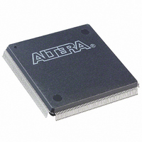
EP1C6Q240I7N Altera, EP1C6Q240I7N Datasheet - Page 82

EP1C6Q240I7N
Manufacturer Part Number
EP1C6Q240I7N
Description
IC CYCLONE FPGA 5980 LE 240-PQFP
Manufacturer
Altera
Series
Cyclone®r
Datasheet
1.EP1C3T144C8.pdf
(106 pages)
Specifications of EP1C6Q240I7N
Number Of Logic Elements/cells
5980
Number Of Labs/clbs
598
Total Ram Bits
92160
Number Of I /o
185
Voltage - Supply
1.425 V ~ 1.575 V
Mounting Type
Surface Mount
Operating Temperature
-40°C ~ 100°C
Package / Case
240-MQFP, 240-PQFP
Family Name
Cyclone®
Number Of Logic Blocks/elements
5980
# I/os (max)
185
Frequency (max)
320.1MHz
Process Technology
0.13um (CMOS)
Operating Supply Voltage (typ)
1.5V
Logic Cells
5980
Ram Bits
92160
Operating Supply Voltage (min)
1.425V
Operating Supply Voltage (max)
1.575V
Operating Temp Range
-40C to 100C
Operating Temperature Classification
Industrial
Mounting
Surface Mount
Pin Count
240
Package Type
PQFP
Lead Free Status / RoHS Status
Lead free / RoHS Compliant
Number Of Gates
-
Lead Free Status / Rohs Status
Compliant
Other names
544-1814
EP1C6Q240I7N
EP1C6Q240I7N
Available stocks
Company
Part Number
Manufacturer
Quantity
Price
Company:
Part Number:
EP1C6Q240I7N
Manufacturer:
ALTERA31
Quantity:
535
Cyclone Device Handbook, Volume 1
4–12
Preliminary
t
t
t
t
t
t
t
t
t
t
t
t
t
t
t
t
t
t
t
t
t
t
t
t
t
t
t
t
SU
H
CO
PIN2COMBOUT_R
PIN2COMBOUT_C
COMBIN2PIN_R
COMBIN2PIN_C
CLR
PRE
CLKHL
M4KRC
M4KWC
M4KWERESU
M4KWEREH
M4KBESU
M4KBEH
M4KDATAASU
M4KDATAAH
M4KADDRASU
M4KADDRAH
M4KDATABSU
M4KDATABH
M4KADDRBSU
M4KADDRBH
M4KDATACO1
M4KDATACO2
M4KCLKHL
M4KCLR
Table 4–22. IOE Internal Timing Microparameter Descriptions
Table 4–23. M4K Block Internal Timing Microparameter Descriptions
Symbol
Symbol
Synchronous read cycle time
Synchronous write cycle time
Write or read enable setup time before clock
Write or read enable hold time after clock
Byte enable setup time before clock
Byte enable hold time after clock
A port data setup time before clock
A port data hold time after clock
A port address setup time before clock
A port address hold time after clock
B port data setup time before clock
B port data hold time after clock
B port address setup time before clock
B port address hold time after clock
Clock-to-output delay when using output registers
Clock-to-output delay without output registers
Minimum clock high or low time
Minimum clear pulse width
IOE input and output register setup time before clock
IOE input and output register hold time after clock
IOE input and output register clock-to-output delay
Row input pin to IOE combinatorial output
Column input pin to IOE combinatorial output
Row IOE data input to combinatorial output pin
Column IOE data input to combinatorial output pin
Minimum clear pulse width
Minimum preset pulse width
Minimum clock high or low time
Parameter
Parameter
Altera Corporation
May 2008


