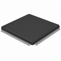
AT40K40AL-1BQU Atmel, AT40K40AL-1BQU Datasheet - Page 14

AT40K40AL-1BQU
Manufacturer Part Number
AT40K40AL-1BQU
Description
FPGA 40K GATE 3.3V 1NS 144-LQFP
Manufacturer
Atmel
Series
AT40KALr
Datasheet
1.AT40K05AL-1AQC.pdf
(55 pages)
Specifications of AT40K40AL-1BQU
Number Of Logic Elements/cells
2304
Total Ram Bits
18432
Number Of I /o
114
Number Of Gates
50000
Voltage - Supply
3 V ~ 3.6 V
Mounting Type
Surface Mount
Operating Temperature
0°C ~ 70°C
Package / Case
144-LQFP
Lead Free Status / RoHS Status
Lead free / RoHS Compliant
Number Of Labs/clbs
-
Available stocks
Company
Part Number
Manufacturer
Quantity
Price
Clocking Scheme
There are eight Global Clock buses (GCK1 - GCK8) on the AT40KAL FPGA. Each of
the eight dedicated Global Clock buses is connected to one of the dual-use Global
Clock pins. Any clocks used in the design should use global clocks where possible: this
can be done by using Assign Pin Locks to lock the clocks to the Global Clock locations.
In addition to the eight Global Clocks, there are four Fast Clocks (FCK1 - FCK4), two per
edge column of the array for PCI specification. For AT40KAL FPGAs, even the derived
clocks can be routed through the Global network. Access points are provided in the cor-
ners of the array to route the derived clocks into the global clock network. The IDS
software tools handle derived clocks to global clock connections automatically if used.
Each column of an array has a “Column Clock mux” and a “Sector Clock mux”. The Col-
umn Clock mux is at the top of every column of an array and the Sector Clock mux is at
every four cells. The Column Clock mux is selected from one of the eight Global Clock
buses. The clock provided to each sector column of four cells is inverted, non-inverted
or tied off to “0”, using the Sector Clock mux to minimize the power consumption in a
sector that has no clocks. The clock can either come from the Column Clock or from the
Plane 4 express bus, see Figure 10 on page 15. The extreme-left Column Clock mux
has two additional inputs, FCK1 and FCK2, to provide fast clocking to left-side I/Os. The
extreme-right Column Clock mux has two additional inputs as well, FCK3 and FCK4, to
provide fast clocking to right-side I/Os.
The register in each cell is triggered on a rising clock edge by default. Before configura-
tion on power-up, constant “0” is provided to each register’s clock pins. After
configuration on power-up, the registers either set or reset, depending on the user’s
choice.
The clocking scheme is designed to allow efficient use of multiple clocks with low clock
skew, both within a column and across the core cell array.
AT40KAL Series FPGA
14
2818F–FPGA–07/06


