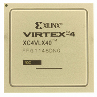
XC4VLX40-10FFG1148C Xilinx Inc, XC4VLX40-10FFG1148C Datasheet - Page 34

XC4VLX40-10FFG1148C
Manufacturer Part Number
XC4VLX40-10FFG1148C
Description
IC FPGA VIRTEX-4 40K 1148-FBGA
Manufacturer
Xilinx Inc
Series
Virtex™-4r
Specifications of XC4VLX40-10FFG1148C
Total Ram Bits
1769472
Number Of Logic Elements/cells
41472
Number Of Labs/clbs
4608
Number Of I /o
640
Voltage - Supply
1.14 V ~ 1.26 V
Mounting Type
Surface Mount
Operating Temperature
0°C ~ 85°C
Package / Case
1148-BBGA, FCBGA
No. Of Logic Blocks
4608
No. Of Macrocells
41472
Family Type
Virtex-4
No. Of Speed Grades
10
No. Of I/o's
640
Clock Management
DCM
Core Supply
RoHS Compliant
Lead Free Status / RoHS Status
Lead free / RoHS Compliant
Number Of Gates
-
Lead Free Status / RoHS Status
Lead free / RoHS Compliant
Other names
122-1491
Available stocks
Company
Part Number
Manufacturer
Quantity
Price
Company:
Part Number:
XC4VLX40-10FFG1148C
Manufacturer:
XILINX
Quantity:
1 238
Company:
Part Number:
XC4VLX40-10FFG1148C
Manufacturer:
Xilinx Inc
Quantity:
10 000
Part Number:
XC4VLX40-10FFG1148C
Manufacturer:
XILINX/赛灵思
Quantity:
20 000
Table 41: FIFO Switching Characteristics
DS302 (v3.7) September 9, 2009
Product Specification
Notes:
1.
2.
3.
4.
5.
6.
7.
Sequential Delays
Setup and Hold Times Before Clock CLK
Reset Delays
Maximum Frequency
T
T
T
T
T
T
F
A Zero “0” Hold Time listing indicates no hold time or a negative hold time. Negative values cannot be guaranteed “best-case,” but if a “0” is listed,
there is no positive hold time.
T
T
T
T
T
T
FCKO_DO
FCKO_FLAGS
FCKO_POINTERS
FDCK_DI
FCCK_EN
FCO_FLAGS
MAX
FCKO_DO
FCKO_FLAGS
FCKO_POINTERS
FDCK_DI
FCCK_EN
FCO_FLAGS
Symbol
/
includes parity inputs (T
/
includes both WRITE and READ enable.
includes parity output (T
T
T
FCKD_DI
includes the following flags: AEMPTY, AFULL, EMPTY, FULL, RDERR, WRERR, RDCOUNT and WRCOUNT.
FCKC_EN
includes the following parameters: T
includes both T
FCKO_RDCOUNT
FDCK_DIP
Clock CLK to DO output
Clock CLK to FIFO flags outputs
Clock CLK to FIFO pointer outputs
DI input
Enable inputs
Reset RST to FLAGS
FIFO in all modes
FCKO_DOP
).
(5)
).
and T
(6)
FCKO_AEMPTY
FCKO_WRCOUNT.
Description
(7)
(2)
www.xilinx.com
, T
FCKO_AFULL
Virtex-4 FPGA Data Sheet: DC and Switching Characteristics
(3)
(4)
, T
FCKO_EMPTY
, T
FCKO_FULL
500.00
0.72
0.93
1.16
0.18
0.26
0.66
0.26
1.32
-12
, T
Speed Grade
FCKO_RDERR
450.45
0.80
1.04
1.29
0.20
0.28
0.73
0.28
1.46
-11
, T
400.00
FCKO_WRERR.
0.92
1.19
1.48
0.23
0.33
0.84
0.33
1.68
-10
ns, Max
ns, Max
ns, Max
ns, Max
ns, Min
ns, Min
Units
MHz
34


