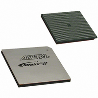
EP2S130F1508C5N Altera, EP2S130F1508C5N Datasheet - Page 140

EP2S130F1508C5N
Manufacturer Part Number
EP2S130F1508C5N
Description
IC STRATIX II FPGA 130K 1508FBGA
Manufacturer
Altera
Series
Stratix® IIr
Datasheet
1.EP2S15F484I4N.pdf
(238 pages)
Specifications of EP2S130F1508C5N
Number Of Logic Elements/cells
132540
Number Of Labs/clbs
6627
Total Ram Bits
6747840
Number Of I /o
1126
Voltage - Supply
1.15 V ~ 1.25 V
Mounting Type
Surface Mount
Operating Temperature
0°C ~ 85°C
Package / Case
1508-FBGA
Lead Free Status / RoHS Status
Lead free / RoHS Compliant
Number Of Gates
-
Other names
544-1871
EP2S130F1508C5N
EP2S130F1508C5N
Available stocks
Company
Part Number
Manufacturer
Quantity
Price
Company:
Part Number:
EP2S130F1508C5N
Manufacturer:
ALTERA
Quantity:
3 000
Part Number:
EP2S130F1508C5N
Manufacturer:
ALTERA/阿尔特拉
Quantity:
20 000
- Current page: 140 of 238
- Download datasheet (3Mb)
Operating Conditions
5–4
Stratix II Device Handbook, Volume 1
Notes to
(1)
(2)
(3)
(4)
I
R
V
V
V
V
Symbol
CCI00
Table 5–4. Stratix II Device DC Operating Conditions (Part 2 of 2)
Table 5–5. LVTTL Specifications (Part 1 of 2)
CCIO
I H
IL
OH
CONF
Symbol
Typical values are for T
This value is specified for normal device operation. The value may vary during power-up. This applies for all
V
Maximum values depend on the actual T
Estimator (available at www.altera.com) or the Quartus II PowerPlay Power Analyzer feature for maximum
values. See the section
Pin pull-up resistance values are lower if an external source drives the pin higher than V
(1)
CCIO
(4)
Table
settings (3.3, 2.5, 1.8, and 1.5 V).
V
(standby)
Value of I/O pin pull-up
resistor before and
during configuration
Recommended value of
I/O pin external
pull-down resistor before
and during configuration
CCIO
Output supply voltage
High-level input voltage
Low-level input voltage
High-level output voltage
5–4:
supply current
Parameter
Parameter
“Power Consumption” on page 5–20
A
= 25°C, V
I/O Standard Specifications
Tables 5–5
specifications.
V
load, no toggling
inputs
T
Vi = 0; V
Vi = 0; V
Vi = 0; V
Vi = 0; V
Vi = 0; V
CCINT
J
I
= ground, no
= 25° C
through
= 1.2 V, and V
J
and design utilization. See the Excel-based PowerPlay Early Power
CCIO
CCIO
CCIO
CCIO
CCIO
I
OH
Conditions
= 3.3 V
= 2.5 V
= 1.8 V
= 1.5 V
= 1.2 V
= –4 mA
5–32
Conditions
CCIO
show the Stratix II device family I/O standard
EP2S15
EP2S30
EP2S60
EP2S90
EP2S130
EP2S180
(2)
= 1.5 V, 1.8 V, 2.5 V, and 3.3 V.
for more information.
Minimum Typical Maximum Unit
Note (1)
10
15
30
40
50
Minimum
3.135
–0.3
1.7
2.4
4.0
4.0
4.0
4.0
4.0
4.0
25
35
50
75
90
1
CCIO
Altera Corporation
.
Maximum
3.465
4.0
0.8
100
150
170
(3)
(3)
(3)
(3)
(3)
(3)
50
70
2
April 2011
mA
mA
mA
mA
mA
mA
Unit
kΩ
kΩ
kΩ
kΩ
kΩ
kΩ
V
V
V
V
Related parts for EP2S130F1508C5N
Image
Part Number
Description
Manufacturer
Datasheet
Request
R

Part Number:
Description:
CYCLONE II STARTER KIT EP2C20N
Manufacturer:
Altera
Datasheet:

Part Number:
Description:
CPLD, EP610 Family, ECMOS Process, 300 Gates, 16 Macro Cells, 16 Reg., 16 User I/Os, 5V Supply, 35 Speed Grade, 24DIP
Manufacturer:
Altera Corporation
Datasheet:

Part Number:
Description:
CPLD, EP610 Family, ECMOS Process, 300 Gates, 16 Macro Cells, 16 Reg., 16 User I/Os, 5V Supply, 15 Speed Grade, 24DIP
Manufacturer:
Altera Corporation
Datasheet:

Part Number:
Description:
Manufacturer:
Altera Corporation
Datasheet:

Part Number:
Description:
CPLD, EP610 Family, ECMOS Process, 300 Gates, 16 Macro Cells, 16 Reg., 16 User I/Os, 5V Supply, 30 Speed Grade, 24DIP
Manufacturer:
Altera Corporation
Datasheet:

Part Number:
Description:
High-performance, low-power erasable programmable logic devices with 8 macrocells, 10ns
Manufacturer:
Altera Corporation
Datasheet:

Part Number:
Description:
High-performance, low-power erasable programmable logic devices with 8 macrocells, 7ns
Manufacturer:
Altera Corporation
Datasheet:

Part Number:
Description:
Classic EPLD
Manufacturer:
Altera Corporation
Datasheet:

Part Number:
Description:
High-performance, low-power erasable programmable logic devices with 8 macrocells, 10ns
Manufacturer:
Altera Corporation
Datasheet:

Part Number:
Description:
Manufacturer:
Altera Corporation
Datasheet:

Part Number:
Description:
Manufacturer:
Altera Corporation
Datasheet:

Part Number:
Description:
Manufacturer:
Altera Corporation
Datasheet:

Part Number:
Description:
CPLD, EP610 Family, ECMOS Process, 300 Gates, 16 Macro Cells, 16 Reg., 16 User I/Os, 5V Supply, 25 Speed Grade, 24DIP
Manufacturer:
Altera Corporation
Datasheet:


