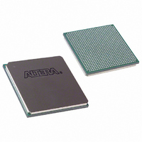
EP1S25F780C5 Altera, EP1S25F780C5 Datasheet - Page 26

EP1S25F780C5
Manufacturer Part Number
EP1S25F780C5
Description
IC STRATIX FPGA 25K LE 780-FBGA
Manufacturer
Altera
Series
Stratix®r
Datasheet
1.EP1S10F780C7.pdf
(276 pages)
Specifications of EP1S25F780C5
Number Of Logic Elements/cells
25660
Number Of Labs/clbs
2566
Total Ram Bits
1944576
Number Of I /o
597
Voltage - Supply
1.425 V ~ 1.575 V
Mounting Type
Surface Mount
Operating Temperature
0°C ~ 85°C
Package / Case
780-FBGA
Family Name
Stratix
Number Of Logic Blocks/elements
25660
# I/os (max)
597
Frequency (max)
500MHz
Process Technology
0.13um (CMOS)
Operating Supply Voltage (typ)
1.5V
Logic Cells
25660
Ram Bits
1944576
Operating Supply Voltage (min)
1.425V
Operating Supply Voltage (max)
1.575V
Operating Temp Range
0C to 85C
Operating Temperature Classification
Commercial
Mounting
Surface Mount
Pin Count
780
Package Type
FC-FBGA
Lead Free Status / RoHS Status
Contains lead / RoHS non-compliant
Number Of Gates
-
Lead Free Status / Rohs Status
Not Compliant
Other names
544-1120
Available stocks
Company
Part Number
Manufacturer
Quantity
Price
Company:
Part Number:
EP1S25F780C5
Manufacturer:
AT
Quantity:
186
Company:
Part Number:
EP1S25F780C5
Manufacturer:
ALTERA
Quantity:
315
Company:
Part Number:
EP1S25F780C5
Manufacturer:
ALTERA
Quantity:
3 000
Company:
Part Number:
EP1S25F780C5AA
Manufacturer:
ALTERA
Quantity:
269
Company:
Part Number:
EP1S25F780C5N
Manufacturer:
ALTERA
Quantity:
3 000
Logic Elements
2–12
Stratix Device Handbook, Volume 1
Figure 2–8
adder. One portion of the LUT generates the sum of two bits using the
input signals and the appropriate carry-in bit; the sum is routed to the
output of the LE. The register can be bypassed for simple adders or used
for accumulator functions. Another portion of the LUT generates carry-
out bits. An LAB-wide carry in bit selects which chain is used for the
addition of given inputs. The carry-in signal for each chain, carry-in0
or carry-in1, selects the carry-out to carry forward to the carry-in
signal of the next-higher-order bit. The final carry-out signal is routed to
an LE, where it is fed to local, row, or column interconnects.
The Quartus II Compiler automatically creates carry chain logic during
design processing, or you can create it manually during design entry.
Parameterized functions such as LPM functions automatically take
advantage of carry chains for the appropriate functions.
The Quartus II Compiler creates carry chains longer than 10 LEs by
linking LABs together automatically. For enhanced fitting, a long carry
chain runs vertically allowing fast horizontal connections to TriMatrix
memory and DSP blocks. A carry chain can continue as far as a full
column.
shows the carry-select circuitry in an LAB for a 10-bit full
Altera Corporation
July 2005
™


