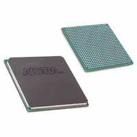
EP2S60F672C3N Altera, EP2S60F672C3N Datasheet - Page 204

EP2S60F672C3N
Manufacturer Part Number
EP2S60F672C3N
Description
IC STRATIX II FPGA 60K 672-FBGA
Manufacturer
Altera
Series
Stratix® IIr
Datasheet
1.EP2S15F484I4N.pdf
(238 pages)
Specifications of EP2S60F672C3N
Number Of Logic Elements/cells
60440
Number Of Labs/clbs
3022
Total Ram Bits
2544192
Number Of I /o
492
Voltage - Supply
1.15 V ~ 1.25 V
Mounting Type
Surface Mount
Operating Temperature
0°C ~ 85°C
Package / Case
672-FBGA
Family Name
Stratix II
Number Of Logic Blocks/elements
60440
# I/os (max)
492
Frequency (max)
816.99MHz
Process Technology
90nm (CMOS)
Operating Supply Voltage (typ)
1.2V
Logic Cells
60440
Ram Bits
2544192
Operating Supply Voltage (min)
1.15V
Operating Supply Voltage (max)
1.25V
Operating Temp Range
0C to 85C
Operating Temperature Classification
Commercial
Mounting
Surface Mount
Pin Count
672
Package Type
FC-FBGA
For Use With
544-1700 - DSP KIT W/STRATIX II EP2S60N544-1697 - NIOS II KIT W/STRATIX II EP2S60N
Lead Free Status / RoHS Status
Lead free / RoHS Compliant
Number Of Gates
-
Lead Free Status / Rohs Status
Compliant
Other names
544-1912
EP2S60F672C3N
EP2S60F672C3N
Available stocks
Company
Part Number
Manufacturer
Quantity
Price
- Current page: 204 of 238
- Download datasheet (3Mb)
Timing Model
5–68
Stratix II Device Handbook, Volume 1
Notes to
(1)
(2)
(3)
(4)
(5)
(6)
1.8-V HSTL Class II
PCI
PCI-X
1.2-V HSTL
Differential SSTL-2 Class I
(1),
Differential SSTL-2 Class II
(1),
Differential SSTL-18 Class I
(1),
Differential SSTL-18 Class II
(1),
1.8-V Differential HSTL
Class I (1),
1.8-V Differential HSTL
Class II (1),
1.5-V Differential HSTL
Class I (1),
1.5-V Differential HSTL
Class II (1),
HyperTransport technology
(4)
LVPECL
LVDS
LVDS
Table 5–77. Maximum Input Toggle Rate on Stratix II Devices (Part 2 of 2)
(3)
(3)
(3)
(3)
(1)
Row clock inputs don’t support PCI, PCI-X, LVPECL, and differential HSTL and SSTL standards.
1.2-V HSTL is only supported on column I/O pins.
Differential HSTL and SSTL standards are only supported on column clock and DQS inputs.
HyperTransport technology is only supported on row I/O and row dedicated clock input pins.
These numbers apply to I/O pins and dedicated clock pins in the left and right I/O banks.
These numbers apply to dedicated clock pins in the top and bottom I/O banks.
Input I/O Standard
(1)
(5)
(6)
Table
(1)
(3)
(3)
(3)
(3)
(2)
5–77:
Column I/O Pins (MHz)
500
500
500
280
500
500
500
500
500
500
500
500
-3
-
-
-
-
500
500
500
500
500
500
500
500
500
500
500
-4
-
-
-
-
-
500
450
450
500
500
500
500
500
500
500
500
-5
-
-
-
-
-
500
520
520
-3
Row I/O Pins (MHz)
-
-
-
-
-
-
-
-
-
-
-
-
-
500
520
520
-4
-
-
-
-
-
-
-
-
-
-
-
-
-
500
420
420
-5
-
-
-
-
-
-
-
-
-
-
-
-
-
Dedicated Clock Inputs
500
500
500
280
500
500
500
500
500
500
500
500
717
450
717
450
-3
Altera Corporation
(MHz)
500
500
500
500
500
500
500
500
500
500
500
717
450
717
450
-4
-
April 2011
500
400
400
500
500
500
500
500
500
500
500
640
400
640
400
-5
-
Related parts for EP2S60F672C3N
Image
Part Number
Description
Manufacturer
Datasheet
Request
R

Part Number:
Description:
CYCLONE II STARTER KIT EP2C20N
Manufacturer:
Altera
Datasheet:

Part Number:
Description:
CPLD, EP610 Family, ECMOS Process, 300 Gates, 16 Macro Cells, 16 Reg., 16 User I/Os, 5V Supply, 35 Speed Grade, 24DIP
Manufacturer:
Altera Corporation
Datasheet:

Part Number:
Description:
CPLD, EP610 Family, ECMOS Process, 300 Gates, 16 Macro Cells, 16 Reg., 16 User I/Os, 5V Supply, 15 Speed Grade, 24DIP
Manufacturer:
Altera Corporation
Datasheet:

Part Number:
Description:
Manufacturer:
Altera Corporation
Datasheet:

Part Number:
Description:
CPLD, EP610 Family, ECMOS Process, 300 Gates, 16 Macro Cells, 16 Reg., 16 User I/Os, 5V Supply, 30 Speed Grade, 24DIP
Manufacturer:
Altera Corporation
Datasheet:

Part Number:
Description:
High-performance, low-power erasable programmable logic devices with 8 macrocells, 10ns
Manufacturer:
Altera Corporation
Datasheet:

Part Number:
Description:
High-performance, low-power erasable programmable logic devices with 8 macrocells, 7ns
Manufacturer:
Altera Corporation
Datasheet:

Part Number:
Description:
Classic EPLD
Manufacturer:
Altera Corporation
Datasheet:

Part Number:
Description:
High-performance, low-power erasable programmable logic devices with 8 macrocells, 10ns
Manufacturer:
Altera Corporation
Datasheet:

Part Number:
Description:
Manufacturer:
Altera Corporation
Datasheet:

Part Number:
Description:
Manufacturer:
Altera Corporation
Datasheet:

Part Number:
Description:
Manufacturer:
Altera Corporation
Datasheet:

Part Number:
Description:
CPLD, EP610 Family, ECMOS Process, 300 Gates, 16 Macro Cells, 16 Reg., 16 User I/Os, 5V Supply, 25 Speed Grade, 24DIP
Manufacturer:
Altera Corporation
Datasheet:


