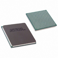
EP1S40F780C7 Altera, EP1S40F780C7 Datasheet - Page 64

EP1S40F780C7
Manufacturer Part Number
EP1S40F780C7
Description
IC STRATIX FPGA 40K LE 780-FBGA
Manufacturer
Altera
Series
Stratix®r
Datasheet
1.EP1S10F780C7.pdf
(276 pages)
Specifications of EP1S40F780C7
Number Of Logic Elements/cells
41250
Number Of Labs/clbs
4125
Total Ram Bits
3423744
Number Of I /o
615
Voltage - Supply
1.425 V ~ 1.575 V
Mounting Type
Surface Mount
Operating Temperature
0°C ~ 85°C
Package / Case
780-FBGA
Lead Free Status / RoHS Status
Contains lead / RoHS non-compliant
Number Of Gates
-
Other names
544-1429
EP1S40SF780C7
EP1S40SF780C7
Available stocks
Company
Part Number
Manufacturer
Quantity
Price
Company:
Part Number:
EP1S40F780C7
Manufacturer:
ALTERA
Quantity:
355
Company:
Part Number:
EP1S40F780C7
Manufacturer:
ALTERA
Quantity:
648
Part Number:
EP1S40F780C7
Manufacturer:
ALTERA/阿尔特拉
Quantity:
20 000
- Current page: 64 of 276
- Download datasheet (4Mb)
TriMatrix Memory
Figure 2–27. Read/Write Clock Mode in Simple Dual-Port Mode
Notes to
(1)
(2)
2–50
Stratix Device Handbook, Volume 1
wraddress[ ]
address[ ]
byteena[ ]
outclken
wrclock
rdclock
inclken
All registers shown except the rden register have asynchronous clear ports.
Violating the setup or hold time on the address registers could corrupt the memory contents. This applies to both
read and write operations.
data[ ]
wren
rden
Figure
8 LAB Row
Clocks
8
2–27:
D
ENA
D
ENA
D
ENA
D
ENA
D
ENA
D
ENA
Q
Q
Q
Q
Q
Q
Generator
Pulse
Write
Data In
Read Address
Write Address
Byte Enable
Read Enable
Write Enable
Notes
Memory Block
(1),
1,024 × 4
2,048 × 2
4,096 × 1
Data Out
256 × 16
512 × 8
(2)
D
ENA
Q
Altera Corporation
To MultiTrack
Interconnect
July 2005
Related parts for EP1S40F780C7
Image
Part Number
Description
Manufacturer
Datasheet
Request
R

Part Number:
Description:
CYCLONE II STARTER KIT EP2C20N
Manufacturer:
Altera
Datasheet:

Part Number:
Description:
CPLD, EP610 Family, ECMOS Process, 300 Gates, 16 Macro Cells, 16 Reg., 16 User I/Os, 5V Supply, 35 Speed Grade, 24DIP
Manufacturer:
Altera Corporation
Datasheet:

Part Number:
Description:
CPLD, EP610 Family, ECMOS Process, 300 Gates, 16 Macro Cells, 16 Reg., 16 User I/Os, 5V Supply, 15 Speed Grade, 24DIP
Manufacturer:
Altera Corporation
Datasheet:

Part Number:
Description:
Manufacturer:
Altera Corporation
Datasheet:

Part Number:
Description:
CPLD, EP610 Family, ECMOS Process, 300 Gates, 16 Macro Cells, 16 Reg., 16 User I/Os, 5V Supply, 30 Speed Grade, 24DIP
Manufacturer:
Altera Corporation
Datasheet:

Part Number:
Description:
High-performance, low-power erasable programmable logic devices with 8 macrocells, 10ns
Manufacturer:
Altera Corporation
Datasheet:

Part Number:
Description:
High-performance, low-power erasable programmable logic devices with 8 macrocells, 7ns
Manufacturer:
Altera Corporation
Datasheet:

Part Number:
Description:
Classic EPLD
Manufacturer:
Altera Corporation
Datasheet:

Part Number:
Description:
High-performance, low-power erasable programmable logic devices with 8 macrocells, 10ns
Manufacturer:
Altera Corporation
Datasheet:

Part Number:
Description:
Manufacturer:
Altera Corporation
Datasheet:

Part Number:
Description:
Manufacturer:
Altera Corporation
Datasheet:

Part Number:
Description:
Manufacturer:
Altera Corporation
Datasheet:

Part Number:
Description:
CPLD, EP610 Family, ECMOS Process, 300 Gates, 16 Macro Cells, 16 Reg., 16 User I/Os, 5V Supply, 25 Speed Grade, 24DIP
Manufacturer:
Altera Corporation
Datasheet:


