EP3C10E144C8N Altera, EP3C10E144C8N Datasheet - Page 55
EP3C10E144C8N
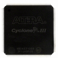
Manufacturer Part Number
EP3C10E144C8N
Description
IC CYCLONE III FPGA 10K 144-EQFP
Manufacturer
Altera
Series
Cyclone® IIIr
Datasheets
1.EP3C5F256C8N.pdf
(5 pages)
2.EP3C5F256C8N.pdf
(34 pages)
3.EP3C5F256C8N.pdf
(66 pages)
4.EP3C5F256C8N.pdf
(14 pages)
5.EP3C5F256C8N.pdf
(76 pages)
6.EP3C10E144C8N.pdf
(274 pages)
Specifications of EP3C10E144C8N
Number Of Logic Elements/cells
10320
Number Of Labs/clbs
645
Total Ram Bits
423936
Number Of I /o
94
Voltage - Supply
1.15 V ~ 1.25 V
Mounting Type
Surface Mount
Operating Temperature
0°C ~ 85°C
Package / Case
144-EQFP
Family Name
Cyclone III
Number Of Logic Blocks/elements
10320
# I/os (max)
94
Frequency (max)
402MHz
Process Technology
65nm
Operating Supply Voltage (typ)
1.2V
Logic Cells
10320
Ram Bits
423936
Operating Supply Voltage (min)
1.15V
Operating Supply Voltage (max)
1.25V
Operating Temp Range
0C to 85C
Operating Temperature Classification
Commercial
Mounting
Surface Mount
Pin Count
144
Package Type
EQFP
For Use With
544-2601 - KIT DEV CYCLONE III LS EP3CLS200544-2411 - KIT DEV NIOS II CYCLONE III ED.
Lead Free Status / RoHS Status
Lead free / RoHS Compliant
Number Of Gates
-
Lead Free Status / Rohs Status
Compliant
Other names
544-2427
EP3C10E144C8N
EP3C10E144C8N
Available stocks
Company
Part Number
Manufacturer
Quantity
Price
Company:

Part Number:
EP3C10E144C8N
Manufacturer:
ALTERA47
Quantity:
516
Part Number:
EP3C10E144C8N
Manufacturer:
ALTERA
Quantity:
20 000


Design Debugging
Design Debugging
© November 2008 Altera Corporation
f
f
You can perform simulation on your Cyclone III design using various simulation
tools. Among the commonly used third-party simulation tools are the Mentor
Graphics ModelSim
ModelSim-Altera edition, ModelSim-Altera web edition as well as the Quartus II
Simulator. Both ModelSim-Altera edition and ModelSim-Altera web edition support
the Cyclone III family.
These third-party simulation tools support functional RTL, post-synthesis and
gate-level simulation. Perform functional RTL simulation before gate-level simulation
or post-synthesis simulation as functional RTL simulation verifies the functionality of
your design before synthesis and place-and-route.
Post-synthesis simulation verifies the functionality of a design after synthesis has
been performed. You can create a post-synthesis netlist in the Quartus II software and
use this netlist to perform post-synthesis simulation with the third-party simulation
tools. After the post-synthesis version of the design is verified, you can then proceed
with the place-and-route for your design in the target Cyclone III device using the
Quartus II Fitter. Use the EDA Netlist Writer of the Quartus II software to generate the
simulation netlist for the specific third-party simulation tool.
Gate-level timing simulation is a post place-and-route simulation to verify the
operation of the design after the worst-case timing delays have been calculated.
Similarly, the Quartus II Simulator supports both functional and timing simulation.
Perform functional simulation at the beginning of your design flow to check the
functionality or logical behavior of your design. You do not need to compile your
design, simply generate the functional simulation netlist of your design which does
not contain timing information to perform functional simulation.
Timing simulation uses the timing netlist generated by the Timing Analyzer when
you compile your design. Timing simulation takes the delay of different device blocks
as well as place-and-route information into consideration, thus is more accurate than
the functional simulation. Perform timing simulation at the top-level design, at the
end of your design flow to ensure that your design works in the targeted device.
For more information about simulating your design with simulation tools, refer to
Simulation
Using incremental compilation when performing on-chip debugging reduces the
compilation time as changes are usually made only to certain parts of the design.
For more information on the on-chip debugging features available in the Quartus II
software, refer to the
Planning” on page
section in volume 3 of the Quartus II Handbook.
3.
®
“Planning for On-Chip Debugging”
, Synopsys VCS and Cadence NC-Sim. You can also use the
section under
“Early System
Page 55
Related parts for EP3C10E144C8N
Image
Part Number
Description
Manufacturer
Datasheet
Request
R

Part Number:
Description:
CYCLONE II STARTER KIT EP2C20N
Manufacturer:
Altera
Datasheet:


Part Number:
Description:
CPLD, EP610 Family, ECMOS Process, 300 Gates, 16 Macro Cells, 16 Reg., 16 User I/Os, 5V Supply, 35 Speed Grade, 24DIP
Manufacturer:
Altera Corporation
Datasheet:
Part Number:
Description:
CPLD, EP610 Family, ECMOS Process, 300 Gates, 16 Macro Cells, 16 Reg., 16 User I/Os, 5V Supply, 15 Speed Grade, 24DIP
Manufacturer:
Altera Corporation
Datasheet:
Part Number:
Description:
Manufacturer:
Altera Corporation
Datasheet:
Part Number:
Description:
CPLD, EP610 Family, ECMOS Process, 300 Gates, 16 Macro Cells, 16 Reg., 16 User I/Os, 5V Supply, 30 Speed Grade, 24DIP
Manufacturer:
Altera Corporation
Datasheet:
Part Number:
Description:
High-performance, low-power erasable programmable logic devices with 8 macrocells, 10ns
Manufacturer:
Altera Corporation
Datasheet:
Part Number:
Description:
High-performance, low-power erasable programmable logic devices with 8 macrocells, 7ns
Manufacturer:
Altera Corporation
Datasheet:
Part Number:
Description:
Classic EPLD
Manufacturer:
Altera Corporation
Datasheet:
Part Number:
Description:
High-performance, low-power erasable programmable logic devices with 8 macrocells, 10ns
Manufacturer:
Altera Corporation
Datasheet:
Part Number:
Description:
Manufacturer:
Altera Corporation
Datasheet:
Part Number:
Description:
Manufacturer:
Altera Corporation
Datasheet:
Part Number:
Description:
Manufacturer:
Altera Corporation
Datasheet:
Part Number:
Description:
CPLD, EP610 Family, ECMOS Process, 300 Gates, 16 Macro Cells, 16 Reg., 16 User I/Os, 5V Supply, 25 Speed Grade, 24DIP
Manufacturer:
Altera Corporation
Datasheet: