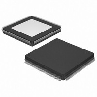
XC3S200-4PQG208C Xilinx Inc, XC3S200-4PQG208C Datasheet - Page 57

XC3S200-4PQG208C
Manufacturer Part Number
XC3S200-4PQG208C
Description
IC SPARTAN-3 FPGA 200K 208-PQFP
Manufacturer
Xilinx Inc
Series
Spartan™-3r
Datasheet
1.XC3S50-4VQG100C.pdf
(217 pages)
Specifications of XC3S200-4PQG208C
Total Ram Bits
221184
Number Of Logic Elements/cells
4320
Number Of Labs/clbs
480
Number Of I /o
141
Number Of Gates
200000
Voltage - Supply
1.14 V ~ 1.26 V
Mounting Type
Surface Mount
Operating Temperature
0°C ~ 85°C
Package / Case
208-BFQFP
No. Of Logic Blocks
480
No. Of Gates
200000
No. Of Macrocells
4320
Family Type
Spartan-3
No. Of Speed Grades
4
No. Of I/o's
141
Clock
RoHS Compliant
Lead Free Status / RoHS Status
Lead free / RoHS Compliant
Other names
122-1339
Available stocks
Company
Part Number
Manufacturer
Quantity
Price
Company:
Part Number:
XC3S200-4PQG208C
Manufacturer:
XILINX/42
Quantity:
1 640
Part Number:
XC3S200-4PQG208C
Manufacturer:
XILINX/赛灵思
Quantity:
20 000
- Current page: 57 of 217
- Download datasheet (6Mb)
Table 29: Power Voltage Ramp Time Requirements
Table 30: Power Voltage Levels Necessary for Preserving RAM Contents
DS099-3 (v2.5) December 4, 2009
Product Specification
98
Notes:
1.
2.
3.
4.
5.
Notes:
1.
2.
3.
Symbol
T
Symbol
V
V
T
If a limit exists, this specification is based on characterization.
The ramp time is measured from 10% to 90% of the full nominal voltage swing for all I/O standards.
For information on power-on current needs, see
For mask revisions earlier than revision E (see
and XC3S400 devices in QFP packages, and limited to 0.6 ms for the XC3S200, XC3S400, XC3S1500, and XC3S4000 devices in
the FT and FG packages.
For earlier device versions with the FQ fabrication/process code (see
500 µs.
RAM contents include data stored in CMOS configuration latches.
The level of the V
If a brown-out condition occurs where V
the minimum power-on reset voltage indicated in
CCINT
DRAUX
DRINT
CCO
R
V
V
in three-rail power-on sequence
V
V
CCO
CCINT
CCINT
CCAUX
CCO
ramp time for all eight banks
ramp time, only if V
level required to retain RAM data
level required to retain RAM data
supply has no effect on data retention.
Description
CCAUX
CCINT
Spartan-3 FPGA Family: DC and Switching Characteristics
or V
Mask and Fab Revisions, page
is last
Power-On Behavior, page 52
Table 28
CCINT
Description
www.xilinx.com
drops below the retention voltage, then V
All
All
in order to clear out the device configuration content.
Device
Mask and Fab Revisions, page
All
All
Package
55), T
CCO
No limit
No limit
min is limited to 2.0 ms for the XC3S200
Min
(4)
CCAUX
55), T
No limit
or V
Max
CCINT
CCINT
-
Min
2.0
1.0
(5)
must drop below
max is limited to
Units
Units
V
V
57
Related parts for XC3S200-4PQG208C
Image
Part Number
Description
Manufacturer
Datasheet
Request
R

Part Number:
Description:
IC SPARTAN-3 FPGA 200K 144-TQFP
Manufacturer:
Xilinx Inc
Datasheet:

Part Number:
Description:
SPARTAN-3A FPGA 200K STD 100VQFP
Manufacturer:
Xilinx Inc
Datasheet:

Part Number:
Description:
SPARTAN-3A FPGA 200K STD 100VQFP
Manufacturer:
Xilinx Inc

Part Number:
Description:
SPARTAN-3A FPGA 200K 144-TQFP
Manufacturer:
Xilinx Inc
Datasheet:

Part Number:
Description:
SPARTAN3A FPGA 200K STD 256FTBGA
Manufacturer:
Xilinx Inc
Datasheet:

Part Number:
Description:
IC FPGA SPARTAN 3 144TQFP
Manufacturer:
Xilinx Inc
Datasheet:

Part Number:
Description:
FLASH PROMS
Manufacturer:
Xilinx Inc
Datasheet:

Part Number:
Description:
FIELD PROGRAMMABLE G A
Manufacturer:
Xilinx Inc
Datasheet:

Part Number:
Description:
FPGA Spartan®-3 Family 200K Gates 4320 Cells 630MHz 90nm Technology 1.2V 256-Pin FTBGA
Manufacturer:
Xilinx Inc
Datasheet:

Part Number:
Description:
FPGA Spartan®-3 Family 200K Gates 4320 Cells 630MHz 90nm Technology 1.2V 256-Pin FTBGA
Manufacturer:
Xilinx Inc
Datasheet:

Part Number:
Description:
FPGA Spartan®-3 Family 200K Gates 4320 Cells 630MHz 90nm Technology 1.2V 208-Pin PQFP
Manufacturer:
Xilinx Inc
Datasheet:

Part Number:
Description:
FPGA Spartan®-3 Family 200K Gates 4320 Cells 630MHz 90nm Technology 1.2V 208-Pin PQFP
Manufacturer:
Xilinx Inc
Datasheet:

Part Number:
Description:
FPGA Spartan®-3 Family 200K Gates 4320 Cells 630MHz 90nm Technology 1.2V 144-Pin TQFP
Manufacturer:
Xilinx Inc
Datasheet:

Part Number:
Description:
FPGA Spartan®-3 Family 200K Gates 4320 Cells 630MHz 90nm Technology 1.2V 144-Pin TQFP
Manufacturer:
Xilinx Inc
Datasheet:

Part Number:
Description:
FPGA Spartan®-3 Family 200K Gates 4320 Cells 630MHz 90nm Technology 1.2V 100-Pin VTQFP
Manufacturer:
Xilinx Inc
Datasheet:


