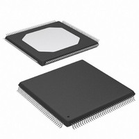
XC3S100E-4TQG144C Xilinx Inc, XC3S100E-4TQG144C Datasheet - Page 200

XC3S100E-4TQG144C
Manufacturer Part Number
XC3S100E-4TQG144C
Description
IC SPARTAN-3E FPGA 100K 144-TQFP
Manufacturer
Xilinx Inc
Series
Spartan™-3Er
Datasheet
1.XC3S100E-4VQG100C.pdf
(233 pages)
Specifications of XC3S100E-4TQG144C
Number Of Logic Elements/cells
2160
Number Of Labs/clbs
240
Total Ram Bits
73728
Number Of I /o
108
Number Of Gates
100000
Voltage - Supply
1.14 V ~ 1.26 V
Mounting Type
Surface Mount
Operating Temperature
0°C ~ 85°C
Package / Case
144-LQFP
Lead Free Status / RoHS Status
Lead free / RoHS Compliant
Other names
122-1478
Available stocks
Company
Part Number
Manufacturer
Quantity
Price
Company:
Part Number:
XC3S100E-4TQG144C
Manufacturer:
XILINX
Quantity:
308
Company:
Part Number:
XC3S100E-4TQG144C
Manufacturer:
Xilinx Inc
Quantity:
10 000
Part Number:
XC3S100E-4TQG144C
Manufacturer:
XILINX/赛灵思
Quantity:
20 000
Pinout Descriptions
User I/Os by Bank
Table
able user-I/O pins are distributed between the four I/O
banks on the FT256 package.
Table 144: User I/Os Per Bank on XC3S250E in the FT256 Package
Table 145: User I/Os Per Bank on XC3S500E in the FT256 Package
.
Table 146: User I/Os Per Bank on XC3S1200E in the FT256 Package
200
Notes:
1.
2.
Notes:
1.
2.
Notes:
1.
2.
Top
Right
Bottom
Left
TOTAL
Top
Right
Bottom
Left
TOTAL
Top
Right
Bottom
Left
TOTAL
Package
Package
Package
Some VREF and CLK pins are on INPUT pins.
The eight global clock pins in this bank have optional functionality during configuration and are counted in the DUAL column.
Some VREF and CLK pins are on INPUT pins.
The eight global clock pins in this bank have optional functionality during configuration and are counted in the DUAL column.
Some VREF and CLK pins are on INPUT pins.
The eight global clock pins in this bank have optional functionality during configuration and are counted in the DUAL column.
Edge
Edge
Edge
144,
Table
145, and
I/O Bank
I/O Bank
I/O Bank
0
1
2
3
0
1
2
3
0
1
2
3
Table 146
Maximum
Maximum
Maximum
172
190
190
indicate how the avail-
I/O
I/O
I/O
44
42
44
42
46
48
48
48
46
48
48
48
I/O
I/O
I/O
20
10
24
62
22
15
11
28
76
24
14
13
27
78
8
www.xilinx.com
The XC3S250E FPGA in the FT256 package has 18 uncon-
nected balls, labeled with an “N.C.” type. These pins are
also indicated with the black diamond ( ) symbol in
Figure
INPUT
INPUT
INPUT
10
33
10
33
31
7
9
7
7
9
7
8
8
7
8
All Possible I/O Pins by Type
All Possible I/O Pins by Type
All Possible I/O Pins by Type
86.
DUAL
DUAL
DUAL
21
24
46
21
24
46
21
24
46
1
0
1
0
1
0
DS312-4 (v3.8) August 26, 2009
VREF
VREF
VREF
15
19
19
5
4
3
3
5
5
4
5
5
5
4
5
(1)
Product Specification
(1)
(1)
CLK
CLK
CLK
0
0
0
0
0
0
16
16
16
8
8
(2)
(2)
8
8
8
8
(2)
(2)
(2)
(2)
(1)
(1)
(1)
R


