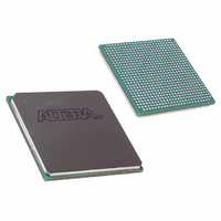
EP2S60F672C5N Altera, EP2S60F672C5N Datasheet - Page 231

EP2S60F672C5N
Manufacturer Part Number
EP2S60F672C5N
Description
IC STRATIX II FPGA 60K 672-FBGA
Manufacturer
Altera
Series
Stratix® IIr
Datasheet
1.EP2S15F484I4N.pdf
(238 pages)
Specifications of EP2S60F672C5N
Number Of Logic Elements/cells
60440
Number Of Labs/clbs
3022
Total Ram Bits
2544192
Number Of I /o
492
Voltage - Supply
1.15 V ~ 1.25 V
Mounting Type
Surface Mount
Operating Temperature
0°C ~ 85°C
Package / Case
672-FBGA
Family Name
Stratix II
Number Of Logic Blocks/elements
60440
# I/os (max)
492
Frequency (max)
609.76MHz
Process Technology
90nm (CMOS)
Operating Supply Voltage (typ)
1.2V
Logic Cells
60440
Ram Bits
2544192
Operating Supply Voltage (min)
1.15V
Operating Supply Voltage (max)
1.25V
Operating Temp Range
0C to 85C
Operating Temperature Classification
Commercial
Mounting
Surface Mount
Pin Count
672
Package Type
FC-FBGA
For Use With
544-1700 - DSP KIT W/STRATIX II EP2S60N544-1697 - NIOS II KIT W/STRATIX II EP2S60N
Lead Free Status / RoHS Status
Lead free / RoHS Compliant
Number Of Gates
-
Lead Free Status / Rohs Status
Compliant
Other names
544-1914
EP2S60F672C5N
EP2S60F672C5N
Available stocks
Company
Part Number
Manufacturer
Quantity
Price
Company:
Part Number:
EP2S60F672C5N
Manufacturer:
ALTERA
Quantity:
238
Part Number:
EP2S60F672C5N
Manufacturer:
ALTERA/阿尔特拉
Quantity:
20 000
- Current page: 231 of 238
- Download datasheet (3Mb)
Altera Corporation
April 2011
Notes to
(1)
(2)
Number of DQS Delay Buffer Stages
Table 5–98. DQS Phase-Shift Error Specifications for DLL-Delayed Clock (tDQS_PSERR)
This error specification is the absolute maximum and minimum error. For example, skew on three delay buffer
stages in a C3 speed grade is 75 ps or ± 37.5 ps
Delay stages used for requested DQS phase shift are reported in your project’s Compilation Report in the
Quartus II software.
Table
5–98:
1
2
3
4
Notes to
(1)
(2)
Note to
(1)
Table 5–97. DQS Phase Jitter Specifications for DLL-Delayed Clock
(tDQS PHASE_JITTER)
Table 5–99. DQS Bus Clock Skew Adder Specifications
(tDQS_CLOCK_SKEW_ADDER)
Number of DQS Delay
Peak-to-peak phase jitter on the phase shifted DDS clock (digital jitter is caused
by DLL tracking).
Delay stages used for requested DQS phase shift are reported in your project’s
Compilation Report in the Quartus II software.
This skew specification is the absolute maximum and minimum skew. For
example, skew on a ×4 DQ group is 40 ps or ±20 ps.
Buffer Stages
×18 DQ per DQS
×36 DQ per DQS
×4 DQ per DQS
×9 DQ per DQS
(2)
Table
Table
Mode
–3 Speed Grade
1
2
3
4
5–99:
5–97:
.
100
25
50
75
(2)
Note (1)
–4 Speed Grade
DQS Phase Jitter
DQS Clock Skew Adder
120
30
60
90
120
30
60
90
Stratix II Device Handbook, Volume 1
40
70
75
95
DC & Switching Characteristics
–5 Speed Grade
105
140
35
70
Unit
ps
ps
ps
ps
(1)
Unit
ps
ps
ps
ps
Unit
ps
ps
ps
ps
5–95
Related parts for EP2S60F672C5N
Image
Part Number
Description
Manufacturer
Datasheet
Request
R

Part Number:
Description:
CYCLONE II STARTER KIT EP2C20N
Manufacturer:
Altera
Datasheet:

Part Number:
Description:
CPLD, EP610 Family, ECMOS Process, 300 Gates, 16 Macro Cells, 16 Reg., 16 User I/Os, 5V Supply, 35 Speed Grade, 24DIP
Manufacturer:
Altera Corporation
Datasheet:

Part Number:
Description:
CPLD, EP610 Family, ECMOS Process, 300 Gates, 16 Macro Cells, 16 Reg., 16 User I/Os, 5V Supply, 15 Speed Grade, 24DIP
Manufacturer:
Altera Corporation
Datasheet:

Part Number:
Description:
Manufacturer:
Altera Corporation
Datasheet:

Part Number:
Description:
CPLD, EP610 Family, ECMOS Process, 300 Gates, 16 Macro Cells, 16 Reg., 16 User I/Os, 5V Supply, 30 Speed Grade, 24DIP
Manufacturer:
Altera Corporation
Datasheet:

Part Number:
Description:
High-performance, low-power erasable programmable logic devices with 8 macrocells, 10ns
Manufacturer:
Altera Corporation
Datasheet:

Part Number:
Description:
High-performance, low-power erasable programmable logic devices with 8 macrocells, 7ns
Manufacturer:
Altera Corporation
Datasheet:

Part Number:
Description:
Classic EPLD
Manufacturer:
Altera Corporation
Datasheet:

Part Number:
Description:
High-performance, low-power erasable programmable logic devices with 8 macrocells, 10ns
Manufacturer:
Altera Corporation
Datasheet:

Part Number:
Description:
Manufacturer:
Altera Corporation
Datasheet:

Part Number:
Description:
Manufacturer:
Altera Corporation
Datasheet:

Part Number:
Description:
Manufacturer:
Altera Corporation
Datasheet:

Part Number:
Description:
CPLD, EP610 Family, ECMOS Process, 300 Gates, 16 Macro Cells, 16 Reg., 16 User I/Os, 5V Supply, 25 Speed Grade, 24DIP
Manufacturer:
Altera Corporation
Datasheet:


