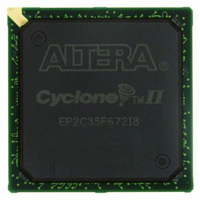
EP2C35F672I8 Altera, EP2C35F672I8 Datasheet - Page 39

EP2C35F672I8
Manufacturer Part Number
EP2C35F672I8
Description
IC CYCLONE II FPGA 33K 672-FBGA
Manufacturer
Altera
Series
Cyclone® IIr
Datasheet
1.EP2C5T144C8N.pdf
(168 pages)
Specifications of EP2C35F672I8
Number Of Logic Elements/cells
33216
Number Of Labs/clbs
2076
Total Ram Bits
483840
Number Of I /o
475
Voltage - Supply
1.15 V ~ 1.25 V
Mounting Type
Surface Mount
Operating Temperature
-40°C ~ 100°C
Package / Case
672-FBGA
Family Name
Cyclone® II
Number Of Logic Blocks/elements
33216
# I/os (max)
475
Frequency (max)
402.58MHz
Process Technology
90nm
Operating Supply Voltage (typ)
1.2V
Logic Cells
33216
Ram Bits
483840
Operating Supply Voltage (min)
1.15V
Operating Supply Voltage (max)
1.25V
Operating Temp Range
-40C to 100C
Operating Temperature Classification
Industrial
Mounting
Surface Mount
Pin Count
672
Package Type
FBGA
For Use With
P0301 - DE2 CALL FOR ACADEMIC PRICING544-1733 - PCI KIT W/CYCLONE II EP2C35N
Lead Free Status / RoHS Status
Contains lead / RoHS non-compliant
Number Of Gates
-
Lead Free Status / Rohs Status
Not Compliant
Other names
544-2110
Available stocks
Company
Part Number
Manufacturer
Quantity
Price
Part Number:
EP2C35F672I8
Manufacturer:
ALTERA
Quantity:
20 000
Company:
Part Number:
EP2C35F672I8N
Manufacturer:
INFINEON
Quantity:
200
Company:
Part Number:
EP2C35F672I8N
Manufacturer:
ALTERA42
Quantity:
201
Part Number:
EP2C35F672I8N
Manufacturer:
ALTERA/阿尔特拉
Quantity:
20 000
Figure 2–16. Cyclone II PLL
Notes to
(1)
(2)
Embedded
Memory
Altera Corporation
February 2007
CLK0 (1)
CLK2 (1)
CLK1
CLK3
This input can be single-ended or differential. If you are using a differential I/O standard, then two CLK pins are
used. LVDS input is supported via the secondary function of the dedicated CLK pins. For example, the CLK0 pin’s
secondary function is LVDSCLK1p and the CLK1 pin’s secondary function is LVDSCLK1n. If a differential I/O
standard is assigned to the PLL clock input pin, the corresponding CLK(n) pin is also completely used. The
Figure 2–16
This counter output is shared between a dedicated external clock output I/O and the global clock network.
Figure
2–16:
shows the possible clock input connections (CLK0/CLK1) to PLL1.
inclk0
inclk1
f
Manual Clock
Select Signal
Switchover
f
IN
Figure 2–16
For more information on Cyclone II PLLs, see the PLLs in the Cyclone II
Devices chapter in Volume 1 of the Cyclone II Device Handbook.
The Cyclone II embedded memory consists of columns of M4K memory
blocks. The M4K memory blocks include input registers that synchronize
writes and output registers to pipeline designs and improve system
performance. The output registers can be bypassed, but input registers
cannot.
÷n
f
Input Clock
REF
f
Reference
FB
Note (1)
= f
IN
/n
PFD
shows a block diagram of the Cyclone II PLL.
down
up
Charge
Pump
Lock Detect
& Filter
÷m
Loop
Filter
Cyclone II Device Handbook, Volume 1
VCO
f
VCO
(3)
÷k
VCO Phase Selection
Selectable at Each
PLL Output Port
8
8
8
Cyclone II Architecture
Post-Scale
Counters
÷c0
÷c1
÷c2
(2)
Global
Clock
Global
Clock
Global
Clock
PLL<#>_OUT
To I/O or
general routing
2–27


