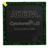
EP2C35F672I8N Altera, EP2C35F672I8N Datasheet - Page 86

EP2C35F672I8N
Manufacturer Part Number
EP2C35F672I8N
Description
IC CYCLONE II FPGA 33K 672-FBGA
Manufacturer
Altera
Series
Cyclone® IIr
Datasheet
1.EP2C5T144C8N.pdf
(168 pages)
Specifications of EP2C35F672I8N
Number Of Logic Elements/cells
33216
Number Of Labs/clbs
2076
Total Ram Bits
483840
Number Of I /o
475
Voltage - Supply
1.15 V ~ 1.25 V
Mounting Type
Surface Mount
Operating Temperature
-40°C ~ 100°C
Package / Case
672-FBGA
Family Name
Cyclone® II
Number Of Logic Blocks/elements
33216
# I/os (max)
475
Frequency (max)
402.58MHz
Process Technology
90nm
Operating Supply Voltage (typ)
1.2V
Logic Cells
33216
Ram Bits
483840
Operating Supply Voltage (min)
1.15V
Operating Supply Voltage (max)
1.25V
Operating Temp Range
-40C to 100C
Operating Temperature Classification
Industrial
Mounting
Surface Mount
Pin Count
672
Package Type
FBGA
For Use With
P0301 - DE2 CALL FOR ACADEMIC PRICING544-1733 - PCI KIT W/CYCLONE II EP2C35N
Lead Free Status / RoHS Status
Lead free / RoHS Compliant
Number Of Gates
-
Lead Free Status / Rohs Status
Compliant
Other names
544-2111
Available stocks
Company
Part Number
Manufacturer
Quantity
Price
Company:
Part Number:
EP2C35F672I8N
Manufacturer:
INFINEON
Quantity:
200
Company:
Part Number:
EP2C35F672I8N
Manufacturer:
ALTERA42
Quantity:
201
Part Number:
EP2C35F672I8N
Manufacturer:
ALTERA/阿尔特拉
Quantity:
20 000
Hot-Socketing Feature Implementation in Cyclone II Devices
Figure 4–1. Hot-Socketing Circuit Block Diagram for Cyclone II Devices
4–4
Cyclone II Device Handbook, Volume 1
Resistor
f
Pull-Up
Weak
PAD
The POR circuit monitors V
tri-stated until the device is in user mode. The weak pull-up resistor (R)
from the I/O pin to V
tolerance control circuit permits the I/O pins to be driven by 3.3 V before
V
driving out when the device is not in user mode.
For more information, see the DC Characteristics & Timing Specifications
chapter in Volume 1 of the Cyclone II Device Handbook for the value of the
internal weak pull-up resistors.
Figure 4–2
I/O buffers. This design ensures that the output buffers do not drive
when V
than V
socketing. The V
circuit capacitance.
R
CCIO
Output
and/or V
CCIO
CCIO
. This also applies for sudden voltage spikes during hot
shows a transistor level cross section of the Cyclone II device
is powered before V
CCINT
PAD
leakage current charges the voltage tolerance control
are powered, and it prevents the I/O pins from
CCIO
Input Buffer
to Logic Array
Tolerance
Voltage
Control
keeps the I/O pins from floating. The voltage
CCINT
CCINT
Output Enable
voltage level and keeps I/O pins
or if the I/O pad voltage is higher
Hot Socket
Pre-Driver
Output
Power-On
Monitor
Reset
Altera Corporation
February 2007


