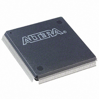
EP2C20Q240C8N Altera, EP2C20Q240C8N Datasheet - Page 95

EP2C20Q240C8N
Manufacturer Part Number
EP2C20Q240C8N
Description
IC CYCLONE II FPGA 20K 240-PQFP
Manufacturer
Altera
Series
Cyclone® IIr
Datasheet
1.EP2C5T144C8N.pdf
(168 pages)
Specifications of EP2C20Q240C8N
Number Of Logic Elements/cells
18752
Number Of Labs/clbs
1172
Total Ram Bits
239616
Number Of I /o
142
Voltage - Supply
1.15 V ~ 1.25 V
Mounting Type
Surface Mount
Operating Temperature
0°C ~ 85°C
Package / Case
240-MQFP, 240-PQFP
Family Name
Cyclone® II
Number Of Logic Blocks/elements
18752
# I/os (max)
142
Frequency (max)
402.58MHz
Process Technology
90nm
Operating Supply Voltage (typ)
1.2V
Logic Cells
18752
Ram Bits
239616
Operating Supply Voltage (min)
1.15V
Operating Supply Voltage (max)
1.25V
Operating Temp Range
0C to 85C
Operating Temperature Classification
Commercial
Mounting
Surface Mount
Pin Count
240
Package Type
PQFP
For Use With
P0528 - BOARD DEV DE1 ALTERA544-1736 - CYCLONE II STARTER KIT EP2C20N
Lead Free Status / RoHS Status
Lead free / RoHS Compliant
Number Of Gates
-
Lead Free Status / Rohs Status
Compliant
Other names
544-2107
Available stocks
Company
Part Number
Manufacturer
Quantity
Price
Company:
Part Number:
EP2C20Q240C8N
Manufacturer:
ALTERA
Quantity:
693
Company:
Part Number:
EP2C20Q240C8N
Manufacturer:
ALTERA
Quantity:
45
Altera Corporation
February 2008
3.3-V LVTTL and
LVCMOS
2.5-V LVTTL and
LVCMOS
1.8-V LVTTL and
LVCMOS
1.5-V LVCMOS
PCI and PCI-X
SSTL-2 class I
SSTL-2 class II
SSTL-18 class I
Table 5–6. Recommended Operating Conditions for User I/O Pins Using Single-Ended I/O Standards
Note (1)
I/O Standard
(Part 1 of 2)
3.135
2.375
1.710
1.425
3.000
2.375
2.375
Min
1.7
V
CCIO
Typ
3.3
2.5
1.8
3.3
2.5
2.5
1.8
1.5
Single-Ended I/O Standards
Tables 5–6
single-ended I/O standards with Cyclone II devices.
descriptions for the voltage and current symbols used in
5–7.
V
V
V
V
V
V
I
I
V
O L
O H
Table 5–5. Voltage and Current Symbol Definitions
C C I O
R E F
I L
I H
O L
O H
T T
(V)
Symbol
3.465
2.625
1.890
1.575
3.600
2.625
2.625
Max
1.9
and
0.833
1.19
1.19
Min
5–7
—
—
—
—
—
Supply voltage for single-ended inputs and for output drivers
Reference voltage for setting the input switching threshold
Input voltage that indicates a low logic level
Input voltage that indicates a high logic level
Output voltage that indicates a low logic level
Output voltage that indicates a high logic level
Output current condition under which V
Output current condition under which V
Voltage applied to a resistor termination as specified by
HSTL and SSTL standards
provide operating condition information when using
V
REF
1.25
1.25
Typ
0.9
—
—
—
—
—
(V)
DC Characteristics and Timing Specifications
0.969
Max
1.31
1.31
—
—
—
—
—
Cyclone II Device Handbook, Volume 1
V
V
V
V
V
V
R E F
R E F
R E F
R E F
R E F
R E F
0.35 × V
0.35 × V
0.3 × V
Definition
– 0.125 (DC)
V
– 0.18 (DC)
– 0.18 (DC)
– 0.35 (AC)
– 0.35 (AC)
– 0.25 (AC)
Max
IL
0.8
0.7
(V)
C C I O
C C I O
C C I O
Table 5–5
O L
O H
V
V
V
V
V
V
R E F
is tested
R E F
R E F
R E F
R E F
R E F
Tables 5–6
is tested
0.65 × V
0.65 × V
0.5 × V
+ 0.125 (DC)
V
+ 0.18 (DC)
+ 0.18 (DC)
+ 0.35 (AC)
+ 0.35 (AC)
+ 0.25 (AC)
Min
IH
1.7
1.7
provides
(V)
C C I O
C C I O
C C I O
and
5–5


